参数资料
| 型号: | IP80C88 |
| 厂商: | Intersil |
| 文件页数: | 33/38页 |
| 文件大小: | 0K |
| 描述: | IC CPU 8/16BIT 5V 5MHZ 40-DIP |
| 标准包装: | 99 |
| 处理器类型: | 80C88 8/16-位 |
| 速度: | 5MHz |
| 电压: | 4.5 ~ 5.5V |
| 安装类型: | 通孔 |
| 封装/外壳: | 40-DIP(0.600",15.24mm) |
| 供应商设备封装: | 40-DIP |
| 包装: | 管件 |
第1页第2页第3页第4页第5页第6页第7页第8页第9页第10页第11页第12页第13页第14页第15页第16页第17页第18页第19页第20页第21页第22页第23页第24页第25页第26页第27页第28页第29页第30页第31页第32页当前第33页第34页第35页第36页第37页第38页
4
FN2949.4
February 22, 2008
Pin Description
The following pin function descriptions are for 80C88 systems in either minimum or maximum mode. The “local bus” in these
descriptions is the direct multiplexed bus interface connection to the 80C88 (without regard to additional bus buffers).
SYMBOL
PIN
NUMBER
TYPE
DESCRIPTION
MAXIMUM OR MINIMUM MODE. THE “LOCAL BUS” IN THESE DESCRIPTIONS IS THE DIRECT MULTIPLEXEDBUS INTERFACE
CONNECTION TO THE 80C88 (WITHOUT REGARD TO ADDITIONAL BUS BUFFERS).
AD7 thru
AD0
9 thru 16
I/O
ADDRESS DATA BUS: These lines constitute the time multiplexed memory/IO address (T1) and data
(T2,T3,Tw and T4) bus. These lines are active HIGH and are held at high impedance to the last valid level
during interrupt acknowledge and local bus “hold acknowledge” or “grant sequence”
A15,
A14 thru A8
39, 2 thru 8
O
ADDRESS BUS: These lines provide address bits 8 through 15 for the entire bus cycle (T1-T4). These
lines do not have to be latched by ALE to remain valid. A15-A8 are active HIGH and are held at high
impedance to the last valid logic level during interrupt acknowledge and local bus “hold acknowledge” or
“grant sequence”.
A19/S6,
A18/S5,
A17/S4,
A16/S3
35
36
37
38
O
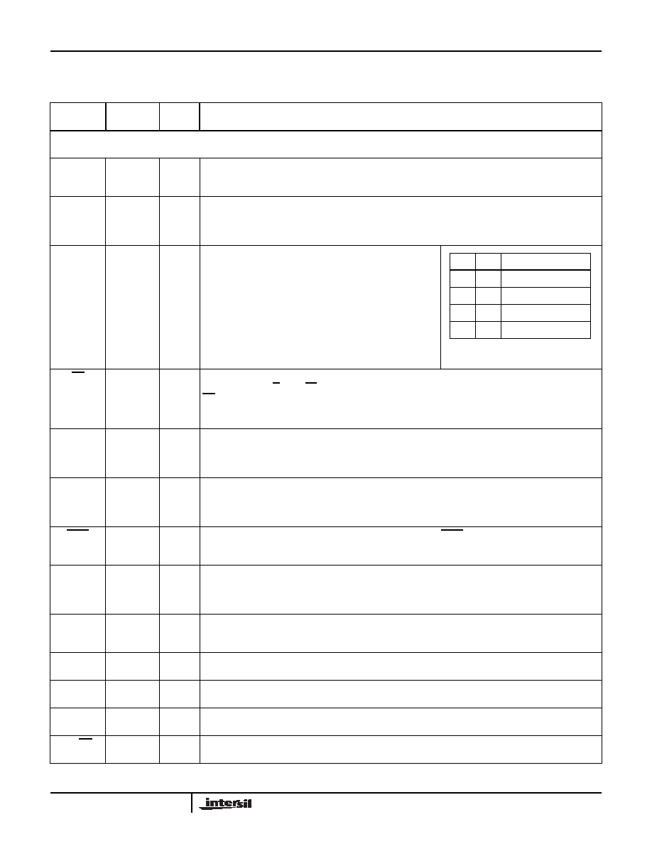
ADDRESS/STATUS: During T1, these are the four most
significant address lines for memory operations. During I/O
operations, these lines are LOW. During memory and I/O
operations, status information is available on these lines during
T2, T3, TW and T4. S6 is always LOW. The status of the
interrupt enable flag bit (S5) is updated at the beginning of each
clock cycle. S4 and S3 are encoded as shown.
This information indicates which segment register is presently
being used for data accessing.
These lines are held at high impedance to the last valid logic
level during local bus “hold acknowledge” or “grant Sequence”.
RD
32
O
READ: Read strobe indicates that the processor is performing a memory or I/O read cycle, depending on
the state of the IO/M pin or S2. This signal is used to read devices which reside on the 80C88 local bus.
RD is active LOW during T2, T3, Tw of any read cycle, and is guaranteed to remain HIGH in T2 until the
80C88 local bus has floated.
This line is held at a high impedance logic one state during “hold acknowledge” or “grant sequence”.
READY
22
I
READY: is the acknowledgment from the address memory or I/O device that it will complete the data
transfer. The RDY signal from memory or I/O is synchronized by the 82C84A clock generator to from
READY. This signal is active HIGH. The 80C88 READY input is not synchronized. Correct operation is not
guaranteed if the set up and hold times are not met.
INTR
18
I
INTERRUPT REQUEST: is a level triggered input which is sampled during the last clock cycle of each
instruction to determine if the processor should enter into an interrupt acknowledge operation. A subroutine
is vectored to via an interrupt vector lookup table located in system memory. It can be internally masked by
software resetting the interrupt enable bit. INTR is internally synchronized. This signal is active HIGH.
TEST
23
I
TEST: input is examined by the “wait for test” instruction. If the TEST input is LOW, execution continues,
otherwise the processor waits in an “idle” state. This input is synchronized internally during each clock cycle
on the leading edge of CLK.
NMI
17
I
NONMASKABLE INTERRUPT: is an edge triggered input which causes a type 2 interrupt. A subroutine is
vectored to via an interrupt vector lookup table located in system memory. NMI is not maskable internally
by software. A transition from a LOW to HIGH initiates the interrupt at the end of the current instruction.
This input is internally synchronized.
RESET
21
I
RESET: cases the processor to immediately terminate its present activity. The signal must transition LOW
to HIGH and remain active HIGH for at least four clock cycles. It restarts execution, as described in the
instruction set description, when RESET returns LOW. RESET is internally synchronized.
CLK
19
I
CLOCK: provides the basic timing for the processor and bus controller. It is asymmetric with a 33% duty
cycle to provide optimized internal timing.
VCC
40
VCC: is the +5V power supply pin. A 0.1F capacitor between pins 20 and 40 recommended for
decoupling.
GND
1, 20
GND: are the ground pins (both pins must be connected to system ground). A 0.1F capacitor between
pins 1 and 20 is recommended for decoupling.
MN/MX
33
I
MINIMUM/MAXIMUM: indicates the mode in which the processor is to operate. The two modes are
discussed in the following sections.
S4
S3
CHARACTERISTICS
0
Alternate Data
01
Stack
1
0
Code or None
11
Data
80C88
相关PDF资料 |
PDF描述 |
|---|---|
| SPC5200CBV400B | IC MPU 32BIT 500MHZ 272PBGA |
| ABB85DHBR | CONN EDGECARD 170PS R/A .050 SLD |
| XF2M-2215-1A | CONN FPC 22POS 0.5MM PITCH SMD |
| MPC859TCVR100A | IC MPU POWERQUICC 100MHZ 357PBGA |
| FMC25DRES | CONN EDGECARD 50POS .100 EYELET |
相关代理商/技术参数 |
参数描述 |
|---|---|
| IP80C88/+ | 制造商:未知厂家 制造商全称:未知厂家 功能描述:16-Bit Microprocessor |
| IP80C88-2 | 功能描述:微处理器 - MPU CPU 8/16BIT 5V 8MHZ IND RoHS:否 制造商:Atmel 处理器系列:SAMA5D31 核心:ARM Cortex A5 数据总线宽度:32 bit 最大时钟频率:536 MHz 程序存储器大小:32 KB 数据 RAM 大小:128 KB 接口类型:CAN, Ethernet, LIN, SPI,TWI, UART, USB 工作电源电压:1.8 V to 3.3 V 最大工作温度:+ 85 C 安装风格:SMD/SMT 封装 / 箱体:FBGA-324 |
| IP80C88-2/+ | 制造商:未知厂家 制造商全称:未知厂家 功能描述:16-Bit Microprocessor |
| IP80C88-2S2064 | 制造商:Rochester Electronics LLC 功能描述:- Bulk |
| IP80C88S2064 | 制造商:Rochester Electronics LLC 功能描述:- Bulk |
发布紧急采购,3分钟左右您将得到回复。