参数资料
| 型号: | IP80C88 |
| 厂商: | Intersil |
| 文件页数: | 36/38页 |
| 文件大小: | 0K |
| 描述: | IC CPU 8/16BIT 5V 5MHZ 40-DIP |
| 标准包装: | 99 |
| 处理器类型: | 80C88 8/16-位 |
| 速度: | 5MHz |
| 电压: | 4.5 ~ 5.5V |
| 安装类型: | 通孔 |
| 封装/外壳: | 40-DIP(0.600",15.24mm) |
| 供应商设备封装: | 40-DIP |
| 包装: | 管件 |
第1页第2页第3页第4页第5页第6页第7页第8页第9页第10页第11页第12页第13页第14页第15页第16页第17页第18页第19页第20页第21页第22页第23页第24页第25页第26页第27页第28页第29页第30页第31页第32页第33页第34页第35页当前第36页第37页第38页
7
FN2949.4
February 22, 2008
Functional Description
Static Operation
All 80C88 circuitry is static in design. Internal registers,
counters and latches are static and require not refresh as
with dynamic circuit design. This eliminates the minimum
operating frequency restriction placed on other
microprocessors. The CMOS 80C88 can operate from DC to
the specified upper frequency limit. The processor clock may
be stopped in either state (high/low) and held there
indefinitely. This type of operation is especially useful for
system debug or power critical applications.
The 80C88 can be single stepped using only the CPU clock.
This state can be maintained as long as is necessary. Single
step clock operation allows simple interface circuitry to
provide critical information for start-up.
Static design also allows very low frequency operation (as
low as DC). In a power critical situation, this can provide
extremely low power operation since 80C88 power
dissipation is directly related to operation frequency. As the
system frequency is reduced, so is the operating power until,
at a DC input frequency, the power requirement is the 80C88
standby current.
Internal Architecture
The internal functions of the 80C88 processor are partitioned
logically into two processing units. The first is the Bus
Interface Unit (BIU) and the second is the Execution Unit
(EU) as shown in the CPU block diagram.
These units can interact directly but for the most part
perform as separate asynchronous operational processors.
The bus interface unit provides the functions related to
instruction fetching and queuing, operand fetch and store,
and address relocation. This unit also provides the basic bus
control. The overlap of instruction pre-fetching provided by
this unit serves to increase processor performance through
improved bus bandwidth utilization. Up to 4-bytes of the
instruction stream can be queued while waiting for decoding
and execution.
The instruction stream queuing mechanism allows the BIU to
keep the memory utilized very efficiently. Whenever there is
space for at least 1-byte in the queue, the BIU will attempt a
byte fetch memory cycle. This greatly reduces “dead time”:
on the memory bus. The queue acts as a First-In-First-Out
(FIFO) buffer, from which the EU extracts instruction bytes
as required. If the queue is empty (following a branch
instruction, for example), the first byte into the queue
immediately becomes available to the EU.
The execution unit receives pre-fetched instructions from the
BIU queue and provides unrelocated operand addresses to
the BIU. Memory operands are passed through the BIU for
processing by the EU, which passes results to the BIU for
storage.
Memory Organization
The processor provides a 20-bit address to memory which
locates the byte being referenced. The memory is organized
as a linear array of up to 1 million bytes, addressed as
00000(H) to FFFFF(H). The memory is logically divided into
code, data, extra, and stack segments of up to 64-bytes
each, with each segment falling on 16-byte boundaries. (See
Figure 1).
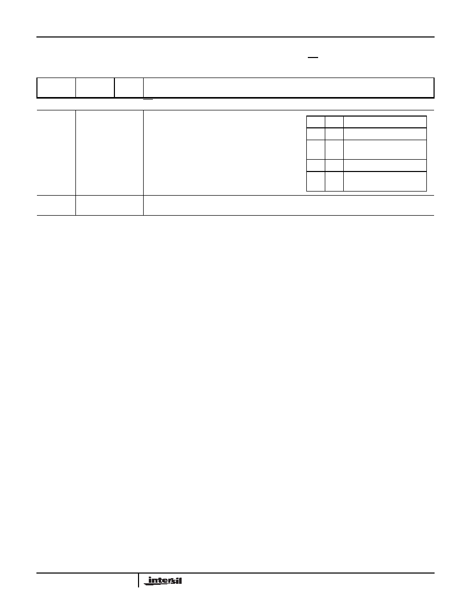
QS1, QS0
24, 25
O
QUEUE STATUS: provide status to allow external
tracking of the internal 80C88 instruction queue.
The queue status is valid during the CLK cycle after
which the queue operation is performed. Note that the
queue status never goes to a high impedance statue
(floated).
34
O
Pin 34 is always a logic one in the maximum mode and is held at a high impedance logic one during a “grant
sequence”.
Pin Description (Continued)
The following pin function descriptions are for 80C88 system in maximum mode (i.e., MN/MX = GND). Only the pin functions which
are unique to the maximum mode are described; all other pin functions are as described above.
SYMBOL
PIN
NUMBER
TYPE
DESCRIPTION
MAXIMUM MODE SYSTEM (i.e., MN/MX = GND).
QS1
QS0
CHARACTERISTICS
00
No Operation
0
1
First Byte of Opcode from
Queue
1
0
Empty the Queue
1
Subsequent Byte from
Queue
80C88
相关PDF资料 |
PDF描述 |
|---|---|
| SPC5200CBV400B | IC MPU 32BIT 500MHZ 272PBGA |
| ABB85DHBR | CONN EDGECARD 170PS R/A .050 SLD |
| XF2M-2215-1A | CONN FPC 22POS 0.5MM PITCH SMD |
| MPC859TCVR100A | IC MPU POWERQUICC 100MHZ 357PBGA |
| FMC25DRES | CONN EDGECARD 50POS .100 EYELET |
相关代理商/技术参数 |
参数描述 |
|---|---|
| IP80C88/+ | 制造商:未知厂家 制造商全称:未知厂家 功能描述:16-Bit Microprocessor |
| IP80C88-2 | 功能描述:微处理器 - MPU CPU 8/16BIT 5V 8MHZ IND RoHS:否 制造商:Atmel 处理器系列:SAMA5D31 核心:ARM Cortex A5 数据总线宽度:32 bit 最大时钟频率:536 MHz 程序存储器大小:32 KB 数据 RAM 大小:128 KB 接口类型:CAN, Ethernet, LIN, SPI,TWI, UART, USB 工作电源电压:1.8 V to 3.3 V 最大工作温度:+ 85 C 安装风格:SMD/SMT 封装 / 箱体:FBGA-324 |
| IP80C88-2/+ | 制造商:未知厂家 制造商全称:未知厂家 功能描述:16-Bit Microprocessor |
| IP80C88-2S2064 | 制造商:Rochester Electronics LLC 功能描述:- Bulk |
| IP80C88S2064 | 制造商:Rochester Electronics LLC 功能描述:- Bulk |
发布紧急采购,3分钟左右您将得到回复。