- 您现在的位置:买卖IC网 > PDF目录383110 > IP82C84A (INTERSIL CORP) CMOS Clock Generator Driver PDF资料下载
参数资料
| 型号: | IP82C84A |
| 厂商: | INTERSIL CORP |
| 元件分类: | XO, clock |
| 英文描述: | CMOS Clock Generator Driver |
| 中文描述: | 8 MHz, PROC SPECIFIC CLOCK GENERATOR, PDIP18 |
| 封装: | PLASTIC, DIP-18 |
| 文件页数: | 4/10页 |
| 文件大小: | 89K |
| 代理商: | IP82C84A |
4-290
Functional Description
Oscillator
The oscillator circuit of the 82C84A is designed primarily for
use with an external parallel resonant, fundamental mode
crystal from which the basic operating frequency is derived.
The crystal frequency should be selected at three times the
required CPU clock. X1 and X2 are the two crystal input
crystal connections. For the most stable operation of the
oscillator (OSC) output circuit, two capacitors (C1 = C2) as
shown in the waveform figures are recommended. The out-
put of the oscillator is buffered and brought out on OSC so
that other system timing signals can be derived from this sta-
ble, crystal-controlled source.
TABLE 1. CRYSTAL SPECIFICATIONS
Capacitors C1, C2 are chosen such that their combined
capacitance
CT =C1 + C2
matches the load capacitance as specified by the crystal
manufacturer. This ensures operation within the frequency
tolerance specified by the crystal manufacturer.
Clock Generator
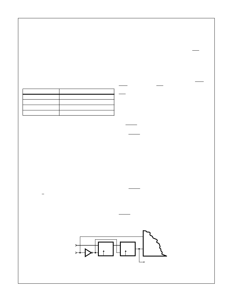
The clock generator consists of a synchronous divide-by-
three counter with a special clear input that inhibits the
counting. This clear input (CSYNC) allows the output clock
to be synchronized with an external event (such as another
82C84A clock). It is necessary to synchronize the CSYNC
input to the EFI clock external to the 82C84A. This is accom-
plished with two flip-flops. (See Figure 1). The counter out-
put is a 33% duty cycle clock at one-third the input
frequency.
NOTE: The F/C input is a strapping pin that selects either the crystal
oscillator or the EFI input as the clock for the
÷
3 counter. If
the EFI input is selected as the clock source, the oscillator
section can be used independently for another clock source.
Output is taken from OSC.
Clock Outputs
The CLK output is a 33% duty cycle clock driver designed to
drive the 80C86, 80C88 processors directly. PCLK is a periph-
eral clock signal whose output frequency is 1/2 that of CLK.
PCLK has a 50% duty cycle.
Reset Logic
The reset logic provides a Schmitt trigger input (RES) and a
synchronizing flip-flop to generate the reset timing. The reset
signal is synchronized to the falling edge of CLK. A simple RC
network can be used to provide power-on reset by utilizing this
function of the 82C84A.
READY Synchronization
Two READY input (RDY1, RDY2) are provided to accommo-
date two system busses. Each input has a qualifier (AEN1 and
AEN2, respectively). The AEN signals validate their respective
RDY signals. If a Multi-Master system is not being used the
AEN pin should be tied LOW.
Synchronization is required for all asynchronous active-going
edges of either RDY input to guarantee that the RDY setup
and hold times are met. Inactive-going edges of RDY in nor-
mally ready systems do not require synchronization but must
satisfy RDY setup and hold as a matter of proper system
design.
The ASYNC input defines two modes of READY synchroniza-
tion operation.
When ASYNC is LOW, two stages of synchronization are pro-
vided for active READY input signals. Positive-going asynchro-
nous READY inputs will first be synchronized to flip-flop one of
the rising edge of CLK (requiring a setup time tR1VCH) and
the synchronized to flip-flop two at the next falling edge of
CLK, after which time the READY output will go active (HIGH).
Negative-going asynchronous READY inputs will be synchro-
nized directly to flip-flop two at the falling edge of CLK, after
which the READY output will go inactive. This mode of opera-
tion is intended for use by asynchronous (normally not ready)
devices in the system which cannot be guaranteed by design
to meet the required RDY setup timing, TR1VCL, on each bus
cycle.
When ASYNC is high or left open, the first READY flip-flop is
bypassed in the READY synchronization logic. READY inputs
are synchronized by flip-flop two on the falling edge of CLK
before they are presented to the processor. This mode is avail-
able for synchronous devices that can be guaranteed to meet
the required RDY setup time.
ASYNC can be changed on every bus cycle to select the
appropriate mode of synchronization for each device in the
system.
PARAMETER
TYPICAL CRYSTAL SPEC
Frequency
2.4 - 25MHz, Fundamental, “AT” cut
Type of Operation
Parallel
Unwanted Modes
6dB (Minimum)
Load Capacitance
18 - 32pF
---------------------
(Including stray capacitance)
EFI
EFI
82C84A
CSYNC
(TO OTHER 82C84As)
CLOCK
SYNCHRONIZE
D
Q
>
D
Q
>
FIGURE 1. CSYNC SYNCHRONIZATION
NOTE: If EFI input is used, then crystal input X1 must be tied to V
CC
or GND and X2 should be left open. If the crystal inputs are used,
then EFI should be tied to V
CC
or GND.
82C84A
相关PDF资料 |
PDF描述 |
|---|---|
| IP82C86H | CMOS Octal Bus Transceiver |
| IP82C86H-5 | CMOS Octal Bus Transceiver |
| IP82C87H | CMOS Octal Inverting Bus Transceiver |
| IP82C87H-5 | CMOS Octal Inverting Bus Transceiver |
| IP82C88 | CMOS Bus Controller |
相关代理商/技术参数 |
参数描述 |
|---|---|
| IP82C86H | 制造商:INTERSIL 制造商全称:Intersil Corporation 功能描述:CMOS Octal Bus Transceiver |
| IP82C86H/+ | 制造商:未知厂家 制造商全称:未知厂家 功能描述:Single 8-bit Bus Transceiver |
| IP82C86H-5 | 制造商:Rochester Electronics LLC 功能描述:- Bulk |
| IP82C87H | 制造商:INTERSIL 制造商全称:Intersil Corporation 功能描述:CMOS Octal Inverting Bus Transceiver |
| IP82C87H/+ | 制造商:未知厂家 制造商全称:未知厂家 功能描述:Single 8-Bit Inverting Bus Transceiver |
发布紧急采购,3分钟左右您将得到回复。