- 您现在的位置:买卖IC网 > PDF目录383110 > IP82C84A (INTERSIL CORP) CMOS Clock Generator Driver PDF资料下载
参数资料
| 型号: | IP82C84A |
| 厂商: | INTERSIL CORP |
| 元件分类: | XO, clock |
| 英文描述: | CMOS Clock Generator Driver |
| 中文描述: | 8 MHz, PROC SPECIFIC CLOCK GENERATOR, PDIP18 |
| 封装: | PLASTIC, DIP-18 |
| 文件页数: | 5/10页 |
| 文件大小: | 89K |
| 代理商: | IP82C84A |
4-291
Absolute Maximum Ratings
Thermal Information
Supply Voltage . . . . . . . . . . . . . . . . . . . . . . . . . . . . . . . . . . . . .+8.0V
Input, Output or I/O Voltage . . . . . . . . . . . GND -0.5V to V
CC
+0.5V
ESD Classification . . . . . . . . . . . . . . . . . . . . . . . . . . . . . . . . Class 1
Operating Conditions
Operating Voltage Range . . . . . . . . . . . . . . . . . . . . . +4.5V to +5.5V
Operating Temperature Range
C82C84A . . . . . . . . . . . . . . . . . . . . . . . . . . . . . . . . 0
o
C to +70
o
C
I82C84A . . . . . . . . . . . . . . . . . . . . . . . . . . . . . . . . -40
o
C to +85
o
C
M82C84A . . . . . . . . . . . . . . . . . . . . . . . . . . . . . . -55
o
C to +125
o
C
Thermal Resistance . . . . . . . . . . . . . . . .
CERDIP Package . . . . . . . . . . . . . . . .
CLCC Package . . . . . . . . . . . . . . . . . .
PDIP Package . . . . . . . . . . . . . . . . . . .
PLCC Package . . . . . . . . . . . . . . . . . .
Storage Temperature Range. . . . . . . . . . . . . . . . . .-65
o
C to +150
o
C
Max Junction Temperature . . . . . . . . . . . . . . . . . . . . . . . . . .+175
o
C
Lead Temperature (Soldering 10s) . . . . . . . . . . . . . . . . . . . .+300
o
C
(PLCC - Lead Tips Only)
θ
JA
(
o
C/W)
80
95
85
85
θ
JC
(
o
C/W)
20
28
N/A
N/A
Die Characteristics
Gate Count . . . . . . . . . . . . . . . . . . . . . . . . . . . . . . . . . . . . .50 Gates
CAUTION: Stresses above those listed in “Absolute Maximum Ratings” may cause permanent damage to the device. This is a stress only rating and operation
of the device at these or any other conditions above those indicated in the operational sections of this specification is not implied.
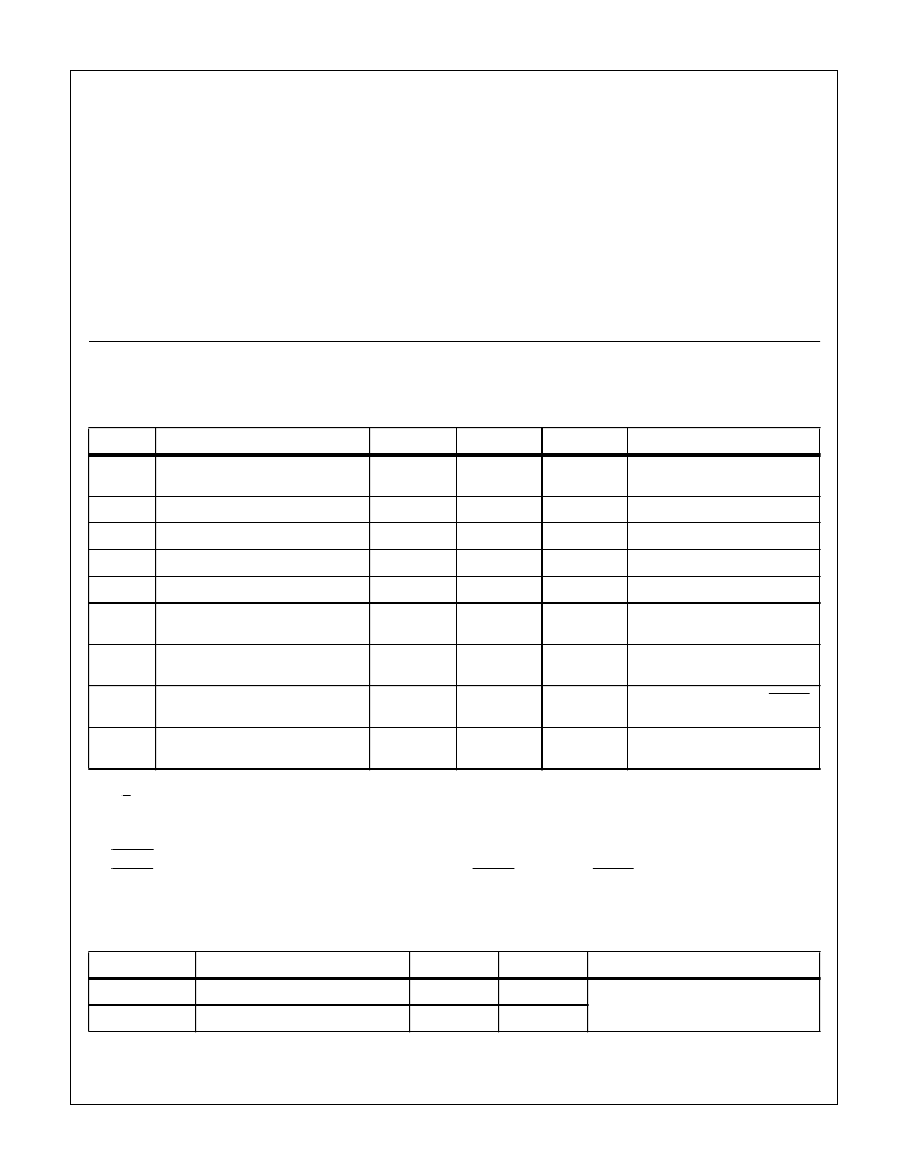
DC Electrical Specifications
V
CC
= +5.0V
±
10%,
T
A
= 0
o
C to +70
o
C (C82C84A),
T
A
= -40
o
C to +85
o
C (I82C84A),
T
A
= -55
o
C to +125
o
C (M82C84A)
SYMBOL
PARAMETER
MIN
MAX
UNITS
TEST CONDITIONS
V
IH
Logical One Input Voltage
2.0
2.2
-
V
V
C82C84A, I82C84
M82C84A, Notes 1, 2
V
IL
Logical Zero Input Voltage
-
0.8
V
Notes 1, 2, 3
V
IHR
Reset Input High Voltage
V
CC
-0.8
-
V
V
ILR
Reset Input Low Voltage
-
0.5
V
VT+ - VT-
Reset Input Hysteresis
0.2 V
CC
-
-
V
OH
Logical One Output Current
V
CC
-0.4
-
V
I
OH
= -4.0mA for CLK Output
I
OH
= -2.5mA for All Others
V
OL
Logical Zero Output Voltage
-
0.4
V
I
OL
= +4.0mA for CLK Output
I
OL
= +2.5mA for All Others
II
Input Leakage Current
-1.0
1.0
μ
A
V
IN
= V
CC
or GND except ASYNC,
X1: (Note 4)
I
CCOP
Operating Power Supply Current
-
40
mA
Crystal Frequency = 25MHz
Outputs Open, Note 5
NOTES:
1. F/C is a strap option and should be held either
≤
0.8V or
≥
2.2V. Does not apply to X1 or X2 pins.
2. Due to test equipment limitations related to noise, the actual tested value may differ from that specified, but the specified limit is
guaranteed.
3. CSYNC pin is tested with V
IL
≤
0.8V.
4. ASYNC pin includes an internal 17.5k
nominal pull-up resistor. For ASYNC input at GND, ASYNC input leakage current = 300
μ
A
nominal, X1 - crystal feedback input.
5. f = 25MHz may be tested using the extrapolated value based on measurements taken at f = 2MHz and f = 10MHz.
Capacitance
T
A
= +25
o
C
SYMBOL
PARAMETER
TYPICAL
UNITS
TEST CONDITIONS
C
IN
Input Capacitance
10
pF
FREQ = 1MHz, all measurements are
referenced to device GND
C
OUT
Output Capacitance
15
pF
82C84A
相关PDF资料 |
PDF描述 |
|---|---|
| IP82C86H | CMOS Octal Bus Transceiver |
| IP82C86H-5 | CMOS Octal Bus Transceiver |
| IP82C87H | CMOS Octal Inverting Bus Transceiver |
| IP82C87H-5 | CMOS Octal Inverting Bus Transceiver |
| IP82C88 | CMOS Bus Controller |
相关代理商/技术参数 |
参数描述 |
|---|---|
| IP82C86H | 制造商:INTERSIL 制造商全称:Intersil Corporation 功能描述:CMOS Octal Bus Transceiver |
| IP82C86H/+ | 制造商:未知厂家 制造商全称:未知厂家 功能描述:Single 8-bit Bus Transceiver |
| IP82C86H-5 | 制造商:Rochester Electronics LLC 功能描述:- Bulk |
| IP82C87H | 制造商:INTERSIL 制造商全称:Intersil Corporation 功能描述:CMOS Octal Inverting Bus Transceiver |
| IP82C87H/+ | 制造商:未知厂家 制造商全称:未知厂家 功能描述:Single 8-Bit Inverting Bus Transceiver |
发布紧急采购,3分钟左右您将得到回复。