- 您现在的位置:买卖IC网 > PDF目录20415 > IR2113S (International Rectifier)IC MOSFET DRVR HI/LO SIDE 16SOIC PDF资料下载
参数资料
| 型号: | IR2113S |
| 厂商: | International Rectifier |
| 文件页数: | 2/18页 |
| 文件大小: | 0K |
| 描述: | IC MOSFET DRVR HI/LO SIDE 16SOIC |
| 标准包装: | 45 |
| 配置: | 高端和低端,独立 |
| 输入类型: | 非反相 |
| 延迟时间: | 120ns |
| 电流 - 峰: | 2.5A |
| 配置数: | 1 |
| 输出数: | 2 |
| 高端电压 - 最大(自引导启动): | 600V |
| 电源电压: | 10 V ~ 20 V |
| 工作温度: | -40°C ~ 125°C |
| 安装类型: | 表面贴装 |
| 封装/外壳: | 16-SOIC(0.295",7.50mm 宽) |
| 供应商设备封装: | 16-SOIC |
| 包装: | 管件 |
| 其它名称: | *IR2113S |
�� �
�
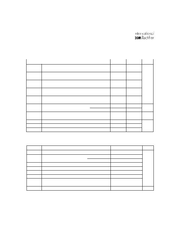
�IR2110(� -� 1� -� 2)(S)PbF/IR2113(� -� 1� -� 2)(S)PbF�
�Absolute� Maximum� Ratings�
�Absolute� maximum� ratings� indicate� sustained� limits� beyond� which� damage� to� the� device� may� occur.� All� voltage� param-�
�eters� are� absolute� voltages� referenced� to� COM.� The� thermal� resistance� and� power� dissipation� ratings� are� measured�
�under� board� mounted� and� still� air� conditions.� Additional� information� is� shown� in� Figures� 28� through� 35.�
�Symbol�
�V� B�
�V� S�
�V� HO�
�V� CC�
�V� LO�
�V� DD�
�V� SS�
�V� IN�
�dV� s� /dt�
�Definition�
�High� side� floating� supply� voltage� (IR2110)�
�(IR2113)�
�High� side� floating� supply� offset� voltage�
�High� side� floating� output� voltage�
�Low� side� fixed� supply� voltage�
�Low� side� output� voltage�
�Logic� supply� voltage�
�Logic� supply� offset� voltage�
�Logic� input� voltage� (HIN,� LIN� &� SD)�
�Allowable� offset� supply� voltage� transient� (figure� 2)�
�Min.�
�-0.3�
�-0.3�
�V� B� -� 25�
�V� S� -� 0.3�
�-0.3�
�-0.3�
�-0.3�
�V� CC� -� 25�
�V� SS� -� 0.3�
�—�
�Max.�
�525�
�625�
�V� B� +� 0.3�
�V� B� +� 0.3�
�25�
�V� CC� +� 0.3�
�V� SS� +� 25�
�V� CC� +� 0.3�
�V� DD� +� 0.3�
�50�
�Units�
�V�
�V/ns�
�P� D�
�R� THJA�
�T� J�
�T� S�
�T� L�
�Package� power� dissipation� @� T� A� ≤� +25� °� C�
�Thermal� resistance,� junction� to� ambient�
�Junction� temperature�
�Storage� temperature�
�Lead� temperature� (soldering,� 10� seconds)�
�(14� lead� DIP)�
�(16� lead� SOIC)�
�(14� lead� DIP)�
�(16� lead� SOIC)�
�—�
�—�
�—�
�—�
�—�
�-55�
�—�
�1.6�
�1.25�
�75�
�100�
�150�
�150�
�300�
�W�
�°� C/W�
�°� C�
�Recommended� Operating� Conditions�
�The� input/output� logic� timing� diagram� is� shown� in� figure� 1.� For� proper� operation� the� device� should� be� used� within� the�
�recommended� conditions.� The� VS� and� VSS� offset� ratings� are� tested� with� all� supplies� biased� at� 15V� differential.� Typical�
�ratings� at� other� bias� conditions� are� shown� in� figures� 36� and� 37.�
�Symbol�
�V� B�
�Definition�
�High� side� floating� supply� absolute� voltage�
�Min.�
�V� S� +� 10�
�Max.�
�V� S� +� 20�
�Units�
�V� S�
�V� HO�
�High� side� floating� supply� offset� voltage�
�High� side� floating� output� voltage�
�(IR2110)�
�(IR2113)�
�Note� 1�
�Note� 1�
�V� S�
�500�
�600�
�V� B�
�V� CC�
�V� LO�
�V� DD�
�V� SS�
�V� IN�
�T� A�
�Low� side� fixed� supply� voltage�
�Low� side� output� voltage�
�Logic� supply� voltage�
�Logic� supply� offset� voltage�
�Logic� input� voltage� (HIN,� LIN� &� SD)�
�Ambient� temperature�
�10�
�0�
�V� SS� +� 3�
�-5� (Note� 2)�
�V� SS�
�-40�
�20�
�V� CC�
�V� SS� +� 20�
�5�
�V� DD�
�125�
�V�
�°� C�
�Note� 1:� Logic� operational� for� V� S� of� -4� to� +500V.� Logic� state� held� for� V� S� of� -4V� to� -V� BS� .� (Please� refer� to� the� Design� Tip�
�DT97-3� for� more� details).�
�Note� 2:� When� V� DD� <� 5V,� the� minimum� V� SS� offset� is� limited� to� -V� DD.�
�2�
�www.irf.com�
�相关PDF资料 |
PDF描述 |
|---|---|
| GCM10DRTN | CONN EDGECARD 20POS DIP .156 SLD |
| LM4050BEM3-4.1+T | IC VREF SHUNT PREC 4.096V SOT23 |
| EBM15DTKN | CONN EDGECARD 30POS DIP .156 SLD |
| ASPI-0418S-150M-T3 | INDUCTOR POWER MINI 15UH 0418 |
| EMM06DTKH | CONN EDGECARD 12POS DIP .156 SLD |
相关代理商/技术参数 |
参数描述 |
|---|---|
| IR2113SPBF | 功能描述:功率驱动器IC HI LO SIDE DRVR 600V 2A 120ns RoHS:否 制造商:Micrel 产品:MOSFET Gate Drivers 类型:Low Cost High or Low Side MOSFET Driver 上升时间: 下降时间: 电源电压-最大:30 V 电源电压-最小:2.75 V 电源电流: 最大功率耗散: 最大工作温度:+ 85 C 安装风格:SMD/SMT 封装 / 箱体:SOIC-8 封装:Tube |
| IR2113STR | 功能描述:IC MOSFET DRVR HI/LO SIDE 16SOIC RoHS:否 类别:集成电路 (IC) >> PMIC - MOSFET,电桥驱动器 - 外部开关 系列:- 标准包装:50 系列:- 配置:低端 输入类型:非反相 延迟时间:40ns 电流 - 峰:9A 配置数:1 输出数:1 高端电压 - 最大(自引导启动):- 电源电压:4.5 V ~ 35 V 工作温度:-40°C ~ 125°C 安装类型:表面贴装 封装/外壳:TO-263-6,D²Pak(5 引线+接片),TO-263BA 供应商设备封装:TO-263 包装:管件 |
| IR2113STRPBF | 功能描述:功率驱动器IC Hi&Lw Sd Drvr All HiVlt Pins 1 Sd RoHS:否 制造商:Micrel 产品:MOSFET Gate Drivers 类型:Low Cost High or Low Side MOSFET Driver 上升时间: 下降时间: 电源电压-最大:30 V 电源电压-最小:2.75 V 电源电流: 最大功率耗散: 最大工作温度:+ 85 C 安装风格:SMD/SMT 封装 / 箱体:SOIC-8 封装:Tube |
| IR21141SSPBF | 功能描述:功率驱动器IC 600V HALF BRDG DRVR IC RoHS:否 制造商:Micrel 产品:MOSFET Gate Drivers 类型:Low Cost High or Low Side MOSFET Driver 上升时间: 下降时间: 电源电压-最大:30 V 电源电压-最小:2.75 V 电源电流: 最大功率耗散: 最大工作温度:+ 85 C 安装风格:SMD/SMT 封装 / 箱体:SOIC-8 封装:Tube |
| IR21141SSPBF_09 | 制造商:IRF 制造商全称:International Rectifier 功能描述:HALF-BRIDGE GATE DRIVER IC |
发布紧急采购,3分钟左右您将得到回复。