- 您现在的位置:买卖IC网 > PDF目录384487 > IR3088AM (International Rectifier) XPHASETM PHASE IC WITH FAULT AND OVERTEMP DETECT PDF资料下载
参数资料
| 型号: | IR3088AM |
| 厂商: | International Rectifier |
| 英文描述: | XPHASETM PHASE IC WITH FAULT AND OVERTEMP DETECT |
| 中文描述: | XPHASETM相集成电路及超温故障检测 |
| 文件页数: | 30/34页 |
| 文件大小: | 1264K |
| 代理商: | IR3088AM |
第1页第2页第3页第4页第5页第6页第7页第8页第9页第10页第11页第12页第13页第14页第15页第16页第17页第18页第19页第20页第21页第22页第23页第24页第25页第26页第27页第28页第29页当前第30页第31页第32页第33页第34页
IR3088A
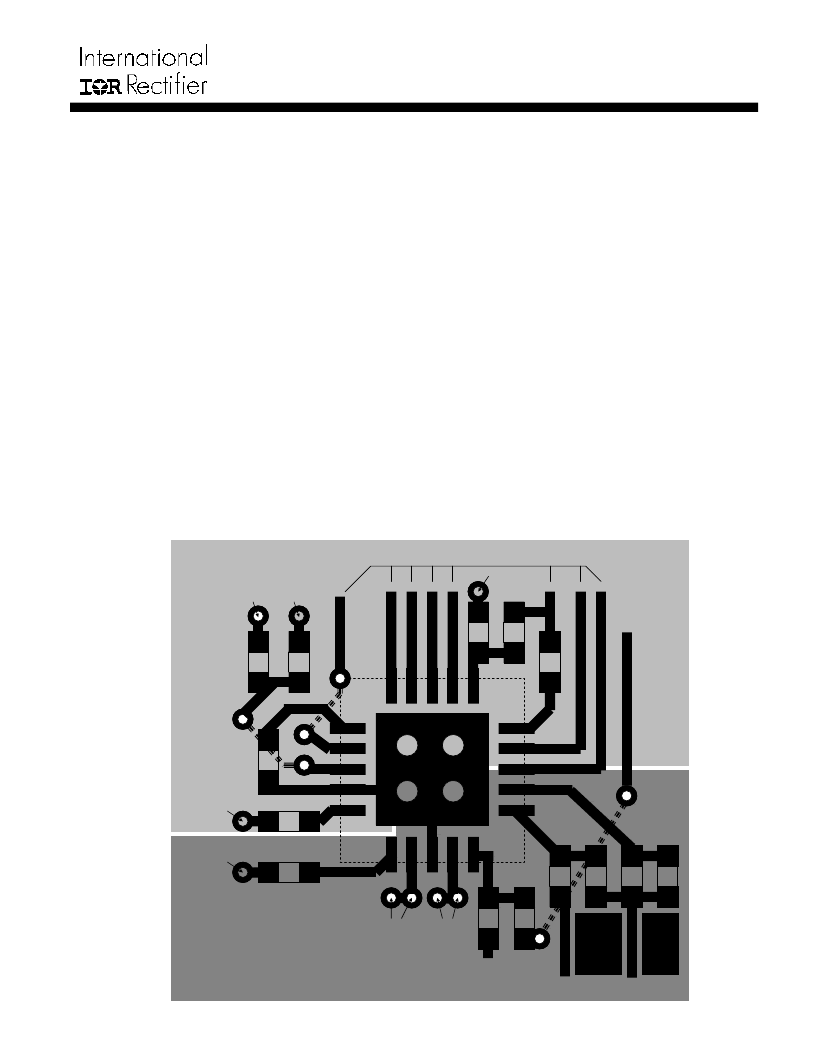
LAYOUT GUIDELINES
The following layout guidelines are recommended to reduce the parasitic inductance and resistance of the PCB
layout, therefore minimizing the noise coupled to the IC.
Dedicate at least one middle layer for a ground plane, which is then split into signal ground plane (LGND) and
power ground plane (PGND).
Connect PGND to LGND pins of each phase IC to the ground tab, which is tied to LGND and PGND planes
respectively through vias.
In order to reduce the noise coupled to SCOMP pin of phase IC, use a dedicated wire to connect the capacitor
C
SCOMP
directly to LGND pin. However, connect PWM ramp capacitor C
PWMRMP
, phase delay programming
resistor R
PHASE2
or R
PHASE3,
decoupling capacitor C
VCC
to LGND plane through vias.
Place current sense resistors and capacitors (R
CS+
, R
CS-
, C
CS+
, and C
CS-
) close to phase IC. Use Kelvin
connection for the inductor current sense wires, but separate the two wires by ground polygon. The wire from
the inductor terminal to RCS- should not cross over the fast transition nodes, i.e. switching nodes, gate drive
outputs and bootstrap nodes.
Place the decoupling capacitors C
VCC
and C
VCCL
as close as possible to VCC and VCCL pins of the phase IC
respectively.
Place the phase IC as close as possible to the MOSFETs to reduce the parasitic resistance and inductance of
the gate drive paths.
Place the input ceramic capacitors close to the drain of top MOSFET and the source of bottom MOSFET. Use
combination of different packages of ceramic capacitors.
There are two switching power loops. One loop includes the input capacitors, top MOSFET, inductor, output
capacitors and the load; another loop consists of bottom MOSFET, inductor, output capacitors and the load.
Route the switching power paths using wide and short traces or polygons; use multiple vias for connections
between layers.
LGND
VCC
SCOMP
CSIN+
CSIN-
DACIN
BIASIN
To Inductor
Plane
Plane
C
VCC
C
VCCL
To VIN
To LGND
Plane
Voltage
PHSFLT
EAIN
PWMRMP
MOSFET
PLANE
To
Node
Polygon
Polygon
Plane
MOSFET
V
E
G
G
P
To Signal Bus
I
To PGND
To LGND
R
P
C
P
C
S
R
B
R
C
D
B
V
C
B
To Gate
Drive
R
P
R
P
V
H
R
R
To Top
PGND
LGND
PLANE
Switching
Ground
C
C
R
C
C
C
Ground
To LGND
To Bottom
Page 30 of 34
9/30
/04
相关PDF资料 |
PDF描述 |
|---|---|
| IR3088AMTR | XPHASETM PHASE IC WITH FAULT AND OVERTEMP DETECT |
| IR3092 | 2 PHASE OPTERON, ATHLON, OR VR10.X CONTROL IC |
| IR3092MTR | 2 PHASE OPTERON, ATHLON, OR VR10.X CONTROL IC |
| IR3220 | FULLY PROTECTED H-BRIDGE FOR D.C. MOTOR |
| IR3500 | XPHASE3TM VR11.0 & AMD PVID CONTROL IC |
相关代理商/技术参数 |
参数描述 |
|---|---|
| IR3088AMPBF | 功能描述:IC XPHASE CONTROL 20L-MLPQ RoHS:是 类别:集成电路 (IC) >> PMIC - 电源管理 - 专用 系列:XPhase™ 应用说明:Ultrasound Imaging Systems Application Note 产品培训模块:Lead (SnPb) Finish for COTS Obsolescence Mitigation Program 标准包装:37 系列:- 应用:医疗用超声波成像,声纳 电流 - 电源:- 电源电压:2.37 V ~ 6 V 工作温度:0°C ~ 70°C 安装类型:表面贴装 封装/外壳:56-WFQFN 裸露焊盘 供应商设备封装:56-TQFN-EP(8x8) 包装:管件 |
| IR3088AMTR | 功能描述:IC XPHASE W/FAULT DET 20L-MLPQ RoHS:否 类别:集成电路 (IC) >> PMIC - 电源管理 - 专用 系列:XPhase™ 应用说明:Ultrasound Imaging Systems Application Note 产品培训模块:Lead (SnPb) Finish for COTS Obsolescence Mitigation Program 标准包装:37 系列:- 应用:医疗用超声波成像,声纳 电流 - 电源:- 电源电压:2.37 V ~ 6 V 工作温度:0°C ~ 70°C 安装类型:表面贴装 封装/外壳:56-WFQFN 裸露焊盘 供应商设备封装:56-TQFN-EP(8x8) 包装:管件 |
| IR3088AMTRPBF | 功能描述:开关变换器、稳压器与控制器 XPHASE IC W/ FAULT OVERTEMP DETECT RoHS:否 制造商:Texas Instruments 输出电压:1.2 V to 10 V 输出电流:300 mA 输出功率: 输入电压:3 V to 17 V 开关频率:1 MHz 工作温度范围: 安装风格:SMD/SMT 封装 / 箱体:WSON-8 封装:Reel |
| IR3088APBF | 制造商:IRF 制造商全称:International Rectifier 功能描述:XPHASETM PHASE IC WITH FAULT AND OVERTEMP DETECT |
| IR3088M | 功能描述:IC XPHASE W/FAULT DET 20L-MLPQ RoHS:否 类别:集成电路 (IC) >> PMIC - 电源管理 - 专用 系列:XPhase™ 应用说明:Ultrasound Imaging Systems Application Note 产品培训模块:Lead (SnPb) Finish for COTS Obsolescence Mitigation Program 标准包装:37 系列:- 应用:医疗用超声波成像,声纳 电流 - 电源:- 电源电压:2.37 V ~ 6 V 工作温度:0°C ~ 70°C 安装类型:表面贴装 封装/外壳:56-WFQFN 裸露焊盘 供应商设备封装:56-TQFN-EP(8x8) 包装:管件 |
发布紧急采购,3分钟左右您将得到回复。