- 您现在的位置:买卖IC网 > PDF目录1810 > IR3870MTRPBF (International Rectifier)IC REG BUCK SYNC ADJ 10A 15QFN PDF资料下载
参数资料
| 型号: | IR3870MTRPBF |
| 厂商: | International Rectifier |
| 文件页数: | 13/20页 |
| 文件大小: | 0K |
| 描述: | IC REG BUCK SYNC ADJ 10A 15QFN |
| 产品培训模块: | SupIRBuck? Family and POL Design Tools Overview |
| 标准包装: | 4,000 |
| 系列: | SupIRBuck™ |
| 类型: | 降压(降压) |
| 输出类型: | 可调式 |
| 输出数: | 1 |
| 输出电压: | 0.5 V ~ 12 V |
| 输入电压: | 3 V ~ 26 V |
| 频率 - 开关: | 可调至 1MHz |
| 电流 - 输出: | 10A |
| 同步整流器: | 是 |
| 工作温度: | 0°C ~ 125°C |
| 安装类型: | 表面贴装 |
| 封装/外壳: | 16-PowerVQFN |
| 包装: | 带卷 (TR) |
| 供应商设备封装: | PQFN(5x6) |
�� �
�
�IR3870MPBF�
�Circuit� Description�
�voltage� is� within� regulation� before� four�
�One� can� use� equation� 4� to� find� the� required�
�consecutive� soft-start� cycles,� PGOOD� transitions�
�inductance.� The� main� advantage� of� small�
�HIGH� to� reset� the� counter.�
�inductance� is� increased� inductor� current� slew�
�rate� during� a� load� transient,� which� leads� to� a�
�OVER� VOLTAGE� PROTECTION�
�The� IR3870� monitors� the� voltage� at� the� FB� node.�
�If� the� FB� voltage� is� above� the� over� voltage�
�threshold,� the� gates� are� turned� off� and� the�
�PGOOD� signal� is� pulled� low.� Toggling� VCC� will�
�allow� the� next� start� up.�
�smaller� output� capacitance� requirement� as�
�discussed� in� the� Output� Capacitor� Selection�
�section.� The� draw� back� of� using� smaller�
�inductances� is� increased� switching� power� loss� in�
�upper� MOSFET,� which� reduces� the� system�
�efficiency� and� increases� the� thermal� dissipation�
�as� discussed� in� the� Power� Loss� section.�
�CHARGE� PUMP�
�The� purpose� of� the� charge� pump� is� to� improve�
�the� system� efficiency.� A� combination� of� VCC,� V5�
�and� three� external� components� are� used� to� boost�
�PVCC� up� to� V� CPTH� .� PVCC� drives� the�
�synchronous� MOSFET� and� reduces� the� R� DSON�
�when� compared� to� a� regular� 5V� rail� driver.� The�
�lower� FET� RDSON� reduces� the� conduction�
�power� loss� as� discussed� in� the� Power� Loss�
�section.� The� charge� pump� is� continuously�
�enabled� for� FCCM� =� HIGH.� The� charge� pump�
�circuit� is� disabled� when� FCCM� =� LOW� and� the�
�output� loading� is� less� than� half� of� inductor� current�
�ripple.� In� this� case,� PVCC� is� two� diode� voltages�
�away� from� the� V5� rail.� Therefore,� the� power� loss�
�for� driver� is� reduced.� The� charge� pump� circuit�
�stops� switching� the� CPO� pin� for� PVCC� above�
�V� CPTH� .�
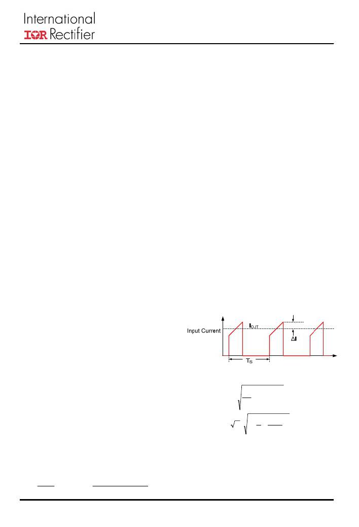
�Input� Capacitor� Selection�
�The� main� function� of� the� input� capacitor� bank� is�
�to� provide� the� input� ripple� current� and� fast� slew�
�rate� current� during� the� load� current� step� up.� The�
�input� capacitor� bank� must� have� adequate� ripple�
�current� carrying� capability� to� handle� the� total�
�RMS� current.� Figure� 16� shows� a� typical� input�
�current.� Equation� 5� shows� the� RMS� input� current.�
�The� RMS� input� current� contains� the� DC� load�
�current� and� the� inductor� ripple� current.� As� shown�
�in� equation� 4,� the� inductor� ripple� current� is�
�unrelated� to� the� load� current.� The� maximum�
�RMS� input� current� occurs� at� the� maximum� output�
�current.� The� maximum� power� dissipation� in� the�
�input� capacitor� equals� the� square� of� the�
�maximum� RMS� input� current� times� the� input�
�capacitor’s� total� ESR.�
�COMPONENT� SELECTION�
�Selection� of� components� for� the� converter� is� an�
�iterative� process� which� involves� meeting� the�
�specifications� and� trade-offs� between� performance�
�and� cost.� The� following� sections� will� guide� one�
�through� the� process.�
�Inductor� Selection�
�Inductor� selection� involves� meeting� the� steady�
�state� output� ripple� requirement,� minimizing� the�
�Figure� 16.� Typical� Input� Current� Waveform.�
�1�
�?� f�
�?� t� ?� ?� dt�
�I� IN_RMS� ?�
�?�
�1� ?� Δ� I� ?�
�switching� loss� of� upper� MOSFETs,� meeting�
�transient� response� specifications� and� minimizing�
�the� output� capacitance.� The� output� voltage�
�includes� a� DC� voltage� and� a� small� AC� ripple�
�component� due� to� the� low� pass� filter� which� has�
�incomplete� attenuation� of� the� switching� harmonics.�
�Neglecting� the� inductance� in� series� with� the� output�
�Ts�
�2�
�Ts�
�0�
�?� I� OUT� ?� D� ?� 1� ?� ?� ?� ?� (5)�
�3� ?� I� OUT� ?�
�2�
�capacitor,� the� magnitude� of� the� AC� voltage� ripple� is�
�determined� by� the� total� inductor� ripple� current� flow�
�through� the� total� equivalent� series� resistance�
�(ESR)� of� the� output� capacitor� bank.�
�The� voltage� rating� of� the� input� capacitor� needs� to� be�
�greater� than� the� maximum� input� voltage� because� of�
�high� frequency� ringing� at� the� phase� node.� The� typical�
�percentage� is� 25%.�
�Δ� I� ?�
�V� OUT�
�L�
�?� ?� 1� ?� D� ?� ?� Ts� ?�
�V� OUT� ?� ?� V� IN� ?� V� OUT� ?�
�V� IN� ?� L� ?� F� s�
�(4)�
�13�
�相关PDF资料 |
PDF描述 |
|---|---|
| IR3871MTR1PBF | IC REG BUCK SYNC ADJ 8A 17QFN |
| IR3876MTRPBF | IC REG BUCK SYNC ADJ 12A 17QFN |
| IR5001SPBF | IC CTRLR/MOSFET UNIV N-CH 8SOIC |
| IR51H310 | IC HALF BRIDGE SELF-OSC 9-SIP |
| IR51HD420 | IC HALF BRIDGE SELF-OSC 9-SIP |
相关代理商/技术参数 |
参数描述 |
|---|---|
| IR3871MPBF | 制造商:IRF 制造商全称:International Rectifier 功能描述:8A HIGHLY INTEGRATED WIDE-INPUT VOLTAGE, SYNCHRONOUS BUCK REGULATOR |
| IR3871MTR1PBF | 功能描述:直流/直流开关调节器 8A SupIRBuck Reg 1000kHz, 3.0-26V in RoHS:否 制造商:International Rectifier 最大输入电压:21 V 开关频率:1.5 MHz 输出电压:0.5 V to 0.86 V 输出电流:4 A 输出端数量: 最大工作温度: 安装风格:SMD/SMT 封装 / 箱体:PQFN 4 x 5 |
| IR3871MTRPBF | 功能描述:直流/直流开关调节器 8A SupIRBuck Reg 1000kHz, 3.0-26V in RoHS:否 制造商:International Rectifier 最大输入电压:21 V 开关频率:1.5 MHz 输出电压:0.5 V to 0.86 V 输出电流:4 A 输出端数量: 最大工作温度: 安装风格:SMD/SMT 封装 / 箱体:PQFN 4 x 5 |
| IR3876MBF | 制造商:IRF 制造商全称:International Rectifier 功能描述:12A HIGHLY INTEGRATED WIDE-INPUT VOLTAGE, SYNCHRONOUS BUCK REGULATOR |
| IR3876MPBF | 制造商:IRF 制造商全称:International Rectifier 功能描述:12A HIGHLY INTEGRATED WIDE-INPUT VOLTAGE, SYNCHRONOUS BUCK REGULATOR |
发布紧急采购,3分钟左右您将得到回复。