- 您现在的位置:买卖IC网 > PDF目录17247 > IRDC3856W (International Rectifier)BOARD EVAL SUPIRBUCK IR3856W PDF资料下载
参数资料
| 型号: | IRDC3856W |
| 厂商: | International Rectifier |
| 文件页数: | 15/34页 |
| 文件大小: | 0K |
| 描述: | BOARD EVAL SUPIRBUCK IR3856W |
| 产品培训模块: | SupIRBuck? Family and POL Design Tools Overview |
| 标准包装: | 1 |
| 系列: | SupIRBuck™ |
| 主要目的: | DC/DC,步降 |
| 输出及类型: | 1,非隔离 |
| 输出电压: | 1.8V |
| 电流 - 输出: | 6A |
| 输入电压: | 12V |
| 稳压器拓扑结构: | 降压 |
| 频率 - 开关: | 600kHz |
| 板类型: | 完全填充 |
| 已供物品: | 板 |
| 已用 IC / 零件: | IR3856W |
第1页第2页第3页第4页第5页第6页第7页第8页第9页第10页第11页第12页第13页第14页当前第15页第16页第17页第18页第19页第20页第21页第22页第23页第24页第25页第26页第27页第28页第29页第30页第31页第32页第33页第34页
�� �
�
�PD-97506�
�IR3856WMPbF�
�Thermal� Shutdown�
�Temperature� sensing� is� provided� inside�
�IR3856W.� The� trip� threshold� is� typically� set� to�
�1.5V� <Vin<16V�
�4.5V� <Vcc<5.5V�
�140� o� C.� When� trip� threshold� is� exceeded,� thermal�
�shutdown� turns� off� both� MOSFETs� and�
�discharges� the� soft� start� capacitor.�
�Automatic� restart� is� initiated� when� the� sensed�
�temperature� drops� within� the� operating� range.�
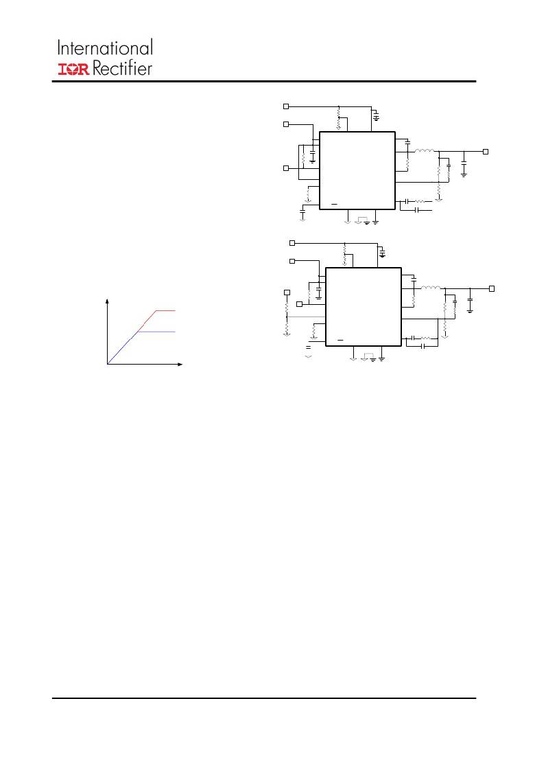
�PGood�
�PVcc�
�Vcc�
�PGood�
�Seq�
�Rt�
�Enable�
�Vin�
�Boot�
�SW�
�OCSet�
�Fb�
�RA�
�RB�
�Vo(master)�
�There� is� a� 20� o� C� hysteresis� in� the� thermal�
�shutdown� threshold.�
�SS/� SD�
�Gnd�
�PGnd�
�Comp�
�Output� Voltage� Sequencing�
�The� IR3856W� can� accommodate� user�
�programmable� sequencing� using� Seq,� Enable�
�1.5V� <Vin<16V�
�4.5V� <Vcc<5.5V�
�and� Power� Good� pins.�
�Vo(master)�
�PVcc�
�Vcc�
�Enable�
�Vin�
�Boot�
�SW�
�Vo(slave)�
�PGood�
�Vo1�
�RE�
�PGood�
�OCSet�
�RC�
�Seq�
�Fb�
�Vo2�
�RF�
�Rt�
�RD�
�SS/� SD�
�Gnd�
�PGnd�
�Comp�
�Simultaneous� Powerup�
�Fig.� 8b.� Application� Circuit� for� Simultaneous�
�Fig.� 8a.� Simultaneous� Power-up� of� the� slave�
�Sequencing�
�with� respect� to� the� master.�
�Power� Good� Output�
�Through� these� pins,� voltage� sequencing� such� as�
�simultaneous� and� sequential� can� be�
�implemented.� Figure� 8.� shows� simultaneous�
�sequencing� configurations.� In� simultaneous�
�power-up,� the� voltage� at� the� Seq� pin� of� the� slave�
�reaches� 0.7V� before� the� Fb� pin� of� the� master.� For�
�R� E� /R� F� =R� C� /R� D� ,� therefore,� the� output� voltage� of�
�the� slave� follows� that� of� the� master� until� the�
�voltage� at� the� Seq� pin� of� the� slave� reaches� 0.7� V.�
�After� the� voltage� at� the� Seq� pin� of� the� slave�
�exceeds� 0.85V,� the� internal� 0.7V� reference� of�
�the� slave� dictates� its� output� voltage.�
�It� is� recommended� that� irrespective� of� the�
�sequencing� configuration� used,� the� input� voltage�
�should� be� allowed� to� come� up� to� its� nominal�
�value� first,� followed� by� V� cc� and� Enable,� before� the�
�sequencing� signal� is� applied.�
�For� non-sequenced� operation,� the� Seq� pin�
�should� be� tied� to� a� voltage� greater� than� 0.85V,�
�such� as� 3.3V� or� V� cc� .� Again,� the� input� voltage�
�should� be� allowed� to� come� up� before� V� cc� and�
�Enable.�
�Rev� 9.0�
�The� IC� continually� monitors� the� output� voltage� via�
�Feedback� (Fb� pin).� The� feedback� voltage� forms�
�an� input� to� a� window� comparator� whose� upper�
�and� lower� thresholds� are� 0.805V� and� 0.595V�
�respectively.� Hence,� the� Power� Good� signal� is�
�flagged� when� the� Fb� pin� voltage� is� within� the�
�PGood� window,� i.� e.� between� 0.595V� to� 0.805V,�
�as� shown� in� Fig� .9.� The� PGood� pin� is� open� drain�
�and� it� needs� to� be� externally� pulled� high.� High�
�state� indicates� that� output� is� in� regulation.� Fig.� 9a�
�shows� the� PGood� timing� diagram� for� non-�
�tracking� operation.� In� this� case,� during� startup,�
�PGood� goes� high� after� the� SS� voltage� reaches�
�2.1V� if� the� Fb� voltage� is� within� the� PGood�
�comparator� window.� Fig.� 9a.� and� Fig� 9.b.� also�
�show� a� 256� cycle� delay� between� the� Fb� voltage�
�entering� within� the� thresholds� defined� by� the�
�PGood� window� and� PGood� going� high.�
�15�
�相关PDF资料 |
PDF描述 |
|---|---|
| HK160868NJ-T | INDUCTOR HI FREQ 68NH 5% 0603 |
| LM4040C25IDBZRG4 | IC VREF SHUNT PREC 2.5V SOT-23-3 |
| ASPI-0804T-102M-T | INDUCTOR POWER 1000UH 0804 SMD |
| RCC18DCSN-S288 | CONN EDGECARD 36POS .100 EXTEND |
| CGRB204-G | DIODE GEN PURP 2A 400V DO-214AA |
相关代理商/技术参数 |
参数描述 |
|---|---|
| IRDC3859 | 功能描述:电源管理IC开发工具 User Guide IR3859 Eval Brd RoHS:否 制造商:Maxim Integrated 产品:Evaluation Kits 类型:Battery Management 工具用于评估:MAX17710GB 输入电压: 输出电压:1.8 V |
| IRDC3859 - SUPIRBUCK | 制造商:International Rectifier 功能描述:INTERNATIONAL RECIFIER - GEN 2.1 SUPIRBUCK FAMILY - Bulk |
| IRDC3859 | 制造商:International Rectifier 功能描述:; MCU Supported Families:IR3859; Feature |
| IRDC3863 | 功能描述:电源管理IC开发工具 9999V 999A POL IC RoHS:否 制造商:Maxim Integrated 产品:Evaluation Kits 类型:Battery Management 工具用于评估:MAX17710GB 输入电压: 输出电压:1.8 V |
| IRDC3865 | 功能描述:电源管理IC开发工具 9999V 999A POL IC RoHS:否 制造商:Maxim Integrated 产品:Evaluation Kits 类型:Battery Management 工具用于评估:MAX17710GB 输入电压: 输出电压:1.8 V |
发布紧急采购,3分钟左右您将得到回复。