- 您现在的位置:买卖IC网 > PDF目录17247 > IRDC3856W (International Rectifier)BOARD EVAL SUPIRBUCK IR3856W PDF资料下载
参数资料
| 型号: | IRDC3856W |
| 厂商: | International Rectifier |
| 文件页数: | 29/34页 |
| 文件大小: | 0K |
| 描述: | BOARD EVAL SUPIRBUCK IR3856W |
| 产品培训模块: | SupIRBuck? Family and POL Design Tools Overview |
| 标准包装: | 1 |
| 系列: | SupIRBuck™ |
| 主要目的: | DC/DC,步降 |
| 输出及类型: | 1,非隔离 |
| 输出电压: | 1.8V |
| 电流 - 输出: | 6A |
| 输入电压: | 12V |
| 稳压器拓扑结构: | 降压 |
| 频率 - 开关: | 600kHz |
| 板类型: | 完全填充 |
| 已供物品: | 板 |
| 已用 IC / 零件: | IR3856W |
第1页第2页第3页第4页第5页第6页第7页第8页第9页第10页第11页第12页第13页第14页第15页第16页第17页第18页第19页第20页第21页第22页第23页第24页第25页第26页第27页第28页当前第29页第30页第31页第32页第33页第34页
�� �
�
�PD-97506�
�IR3856WMPbF�
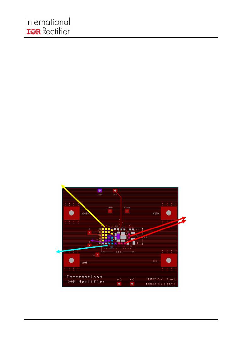
�Layout� Considerations�
�Vin�
�PGnd�
�PGnd�
�capacitor� at� the� Sw� pin.�
�AGnd� Vout�
�The� layout� is� very� important� when� designing� high�
�frequency� switching� converters.� Layout� will� affect�
�noise� pickup� and� can� cause� a� good� design� to�
�perform� with� less� than� expected� results.�
�Make� all� the� connections� for� the� power�
�components� in� the� top� layer� with� wide,� copper�
�filled� areas� or� polygons.� In� general,� it� is� desirable�
�to� make� proper� use� of� power� planes� and�
�polygons� for� power� distribution� and� heat�
�dissipation.�
�The� inductor,� output� capacitors� and� the� IR3856W�
�should� be� as� close� to� each� other� as� possible.�
�This� helps� to� reduce� the� EMI� radiated� by� the�
�power� traces� due� to� the� high� switching� currents�
�through� them.� Place� the� input� capacitor� directly� at�
�the� Vin� pin� of� IR3856W.�
�The� feedback� part� of� the� system� should� be� kept�
�away� from� the� inductor� and� other� noise� sources.�
�The� critical� bypass� components� such� as�
�capacitors� for� Vcc� should� be� close� to� their�
�respective� pins.� It� is� important� to� place� the�
�feedback� components� including� feedback�
�resistors� and� compensation� components� close� to�
�Fb� and� Comp� pins.�
�Compensation� parts�
�should� be� placed� as� close�
�as� possible� to�
�the� Comp� pin� .�
�Vout�
�The� connection� between� the� OCSet� resistor� and�
�the� Sw� pin� should� not� share� any� trace� with� the�
�connection� between� the� bootstrap� capacitor� and�
�the� Sw� pin.� Instead,� it� is� recommended� to� use� a�
�Kelvin� connection� of� the� trace� from� the� OCSet�
�resistor� and� the� trace� from� the� bootstrap�
�Vin�
�VoutAGnd�
�In� a� multilayer� PCB� use� one� layer� as� a� power�
�ground� plane� and� have� a� control� circuit� ground�
�(analog� ground),� to� which� all� signals� are�
�referenced.� The� goal� is� to� localize� the� high�
�current� path� to� a� separate� loop� that� does� not�
�interfere� with� the� more� sensitive� analog� control�
�function.� These� two� grounds� must� be� connected�
�together� on� the� PC� board� layout� at� a� single� point.�
�The� Power� QFN� is� a� thermally� enhanced�
�package.� Based� on� thermal� performance� it� is�
�recommended� to� use� at� least� a� 4-layers� PCB.� To�
�effectively� remove� heat� from� the� device� the�
�exposed� pad� should� be� connected� to� the� ground�
�plane� using� vias.� Figure� 26� illustrates� the�
�implementation� of� the� layout� guidelines� outlined�
�above,� on� the� IRDC3856W� 4� layer� demoboard.�
�Vin�
�All� bypass� caps�
�should� be� placed� as�
�close� as� possible� to�
�their� connecting�
�pins.�
�Resistors� Rt,� Rocset,�
�AGnd�
�Vin�
�and� SS� capacitor�
�should� be� placed� as�
�close� as� possible� to�
�their� pins.�
�PGnd�
�Fig.� 26a.� IRDC3856W� demo-board� layout�
�considerations� –� Top� Layer�
�Rev� 9.0�
�29�
�相关PDF资料 |
PDF描述 |
|---|---|
| HK160868NJ-T | INDUCTOR HI FREQ 68NH 5% 0603 |
| LM4040C25IDBZRG4 | IC VREF SHUNT PREC 2.5V SOT-23-3 |
| ASPI-0804T-102M-T | INDUCTOR POWER 1000UH 0804 SMD |
| RCC18DCSN-S288 | CONN EDGECARD 36POS .100 EXTEND |
| CGRB204-G | DIODE GEN PURP 2A 400V DO-214AA |
相关代理商/技术参数 |
参数描述 |
|---|---|
| IRDC3859 | 功能描述:电源管理IC开发工具 User Guide IR3859 Eval Brd RoHS:否 制造商:Maxim Integrated 产品:Evaluation Kits 类型:Battery Management 工具用于评估:MAX17710GB 输入电压: 输出电压:1.8 V |
| IRDC3859 - SUPIRBUCK | 制造商:International Rectifier 功能描述:INTERNATIONAL RECIFIER - GEN 2.1 SUPIRBUCK FAMILY - Bulk |
| IRDC3859 | 制造商:International Rectifier 功能描述:; MCU Supported Families:IR3859; Feature |
| IRDC3863 | 功能描述:电源管理IC开发工具 9999V 999A POL IC RoHS:否 制造商:Maxim Integrated 产品:Evaluation Kits 类型:Battery Management 工具用于评估:MAX17710GB 输入电压: 输出电压:1.8 V |
| IRDC3865 | 功能描述:电源管理IC开发工具 9999V 999A POL IC RoHS:否 制造商:Maxim Integrated 产品:Evaluation Kits 类型:Battery Management 工具用于评估:MAX17710GB 输入电压: 输出电压:1.8 V |
发布紧急采购,3分钟左右您将得到回复。