- 您现在的位置:买卖IC网 > Datasheet目录443 > IRF510 (Vishay Siliconix)MOSFET N-CH 100V 5.6A TO-220AB Datasheet资料下载
参数资料
| 型号: | IRF510 |
| 厂商: | Vishay Siliconix |
| 文件页数: | 2/9页 |
| 文件大小: | 0K |
| 描述: | MOSFET N-CH 100V 5.6A TO-220AB |
| 标准包装: | 1,000 |
| FET 型: | MOSFET N 通道,金属氧化物 |
| FET 特点: | 标准 |
| 漏极至源极电压(Vdss): | 100V |
| 电流 - 连续漏极(Id) @ 25° C: | 5.6A |
| 开态Rds(最大)@ Id, Vgs @ 25° C: | 540 毫欧 @ 3.4A,10V |
| Id 时的 Vgs(th)(最大): | 4V @ 250µA |
| 闸电荷(Qg) @ Vgs: | 8.3nC @ 10V |
| 输入电容 (Ciss) @ Vds: | 180pF @ 25V |
| 功率 - 最大: | 43W |
| 安装类型: | 通孔 |
| 封装/外壳: | TO-220-3 |
| 供应商设备封装: | TO-220AB |
| 包装: | 管件 |
| 其它名称: | *IRF510 |
�� �
�
�IRF510,� SiHF510�
�Vishay� Siliconix�
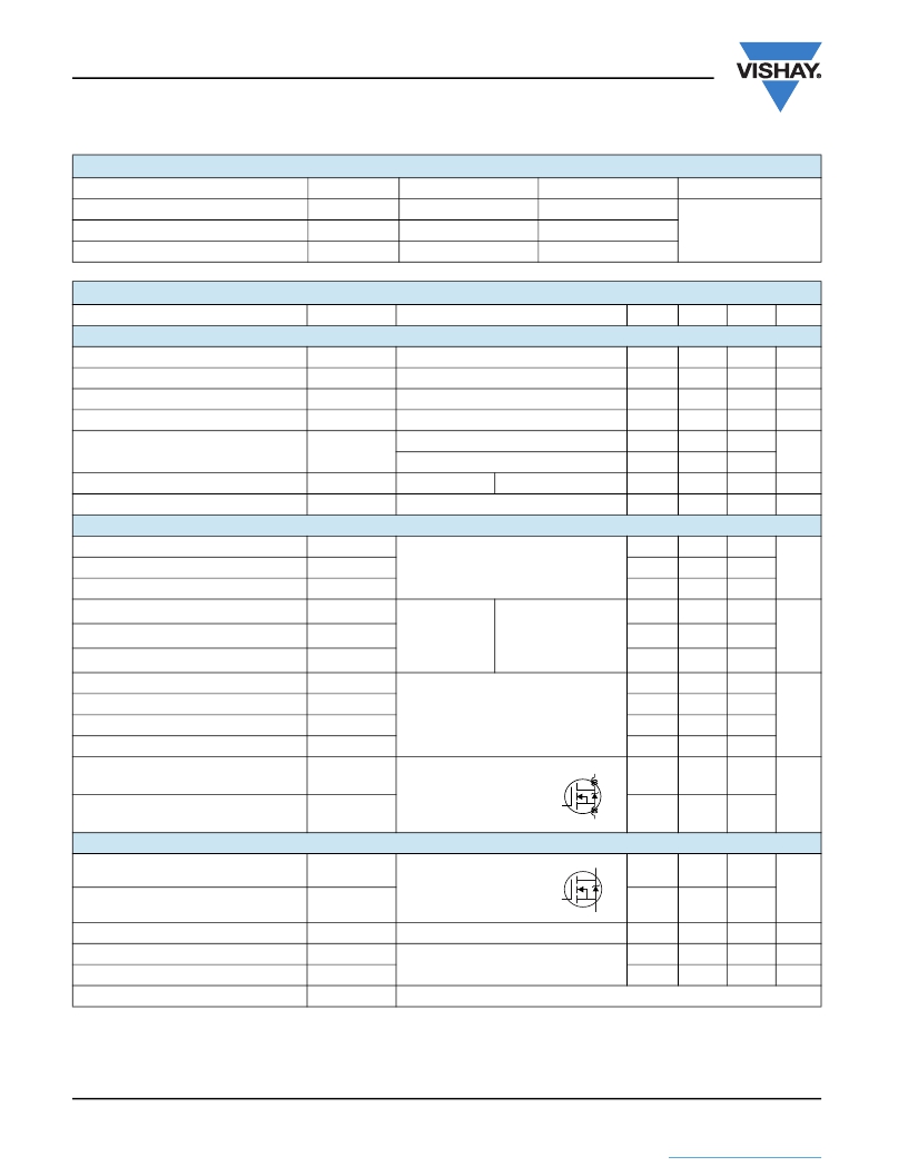
�THERMAL� RESISTANCE� RATINGS�
�PARAMETER�
�Maximum� Junction-to-Ambient�
�Case-to-Sink,� Flat,� Greased� Surface�
�Maximum� Junction-to-Case� (Drain)�
�SYMBOL�
�R� thJA�
�R� thCS�
�R� thJC�
�TYP.�
�-�
�0.50�
�-�
�MAX.�
�62�
�-�
�3.5�
�UNIT�
�°C/W�
�SPECIFICATIONS� (T� J� =� 25� °C,� unless� otherwise� noted)�
�PARAMETER�
�SYMBOL�
�TEST� CONDITIONS�
�MIN.�
�TYP.�
�MAX.�
�UNIT�
�Static�
�Drain-Source� Breakdown� Voltage�
�V� DS� Temperature� Coefficient�
�Gate-Source� Threshold� Voltage�
�Gate-Source� Leakage�
�Zero� Gate� Voltage� Drain� Current�
�V� DS�
�?� V� DS� /T� J�
�V� GS(th)�
�I� GSS�
�I� DSS�
�V� GS� =� 0� V,� I� D� =� 250� μA�
�Reference� to� 25� °C,� I� D� =� 1� mA�
�V� DS� =� V� GS� ,� I� D� =� 250� μA�
�V� GS� =� ±� 20� V�
�V� DS� =� 100� V,� V� GS� =� 0� V�
�V� DS� =� 80� V,� V� GS� =� 0� V,� T� J� =� 150� °C�
�100�
�-�
�2.0�
�-�
�-�
�-�
�-�
�0.12�
�-�
�-�
�-�
�-�
�-�
�-�
�4.0�
�±� 100�
�25�
�250�
�V�
�V/°C�
�V�
�nA�
�μA�
�Drain-Source� On-State� Resistance�
�R� DS(on)�
�V� GS� =� 10� V�
�I� D� =3.4� A� b�
�-�
�-�
�0.54�
�?�
�Forward� Transconductance�
�g� fs�
�V� DS� =� 50� V,� I� D� =� 3.4� A� b�
�1.3�
�-�
�-�
�S�
�Dynamic�
�Input� Capacitance�
�C� iss�
�V� GS� =� 0� V,�
�-�
�180�
�-�
�Output� Capacitance�
�Reverse� Transfer� Capacitance�
�Total� Gate� Charge�
�C� oss�
�C� rss�
�Q� g�
�V� DS� =� 25� V,�
�f� =� 1.0� MHz,� see� fig.� 5�
�I� D� =� 5.6� A,� V� DS� =� 80� V�
�-�
�-�
�-�
�81�
�15�
�-�
�-�
�-�
�8.3�
�pF�
�Gate-Source� Charge�
�Gate-Drain� Charge�
�Q� gs�
�Q� gd�
�V� GS� =� 10� V�
�V� DS� =� 10� V,�
�13� b�
�see� fig.� 6� and�
�-�
�-�
�-�
�-�
�2.3�
�3.8�
�nC�
�Turn-On� Delay� Time�
�t� d(on)�
�-�
�6.9�
�-�
�Rise� Time�
�Turn-Off� Delay� Time�
�Fall� Time�
�t� r�
�t� d(off)�
�t� f�
�V� DD� =� 50� V,� I� D� =� 5.6� A�
�R� g� =� 24� ?� ,� R� D� =� 8.4� ??� ,� see� fig.� 10� b�
�-�
�-�
�-�
�16�
�15�
�9.4�
�-�
�-�
�-�
�ns�
�Internal� Drain� Inductance�
�Internal� Source� Inductance�
�L� D�
�L� S�
�Between� lead,�
�6� mm� (0.25")� from�
�package� and� center� of�
�die� contact�
�G�
�D�
�S�
�-�
�-�
�4.5�
�7.5�
�-�
�-�
�nH�
�Drain-Source� Body� Diode� Characteristics�
�Continuous� Source-Drain� Diode� Current�
�I� S�
�MOSFET� symbol�
�showing� the�
�D�
�-�
�-�
�5.6�
�integral� reverse�
�G�
�A�
�Pulsed� Diode� Forward� Current� a�
�I� SM�
�p� -� n� junction� diode�
�S�
�-�
�-�
�20�
�Body� Diode� Voltage�
�Body� Diode� Reverse� Recovery� Time�
�Body� Diode� Reverse� Recovery� Charge�
�V� SD�
�t� rr�
�Q� rr�
�T� J� =� 25� °C,� I� S� =� 5.6� A,� V� GS� =� 0� V� b�
�T� J� =� 25� °C,� I� F� =� 5.6� A,� dI/dt� =� 100� A/μs� b�
�-�
�-�
�-�
�-�
�100�
�0.44�
�2.5�
�200�
�0.88�
�V�
�ns�
�μC�
�Forward� Turn-On� Time�
�t� on�
�Intrinsic� turn-on� time� is� negligible� (turn-on� is� dominated� by� L� S� and� L� D� )�
�Notes�
�a.� Repetitive� rating;� pulse� width� limited� by� maximum� junction� temperature� (see� fig.� 11).�
�b.� Pulse� width� ?� 300� μs;� duty� cycle� ?� 2� %.�
�www.vishay.com�
�2�
�Document� Number:� 91015�
�S11-0511-Rev.� B,� 21-Mar-11�
�This� datasheet� is� subject� to� change� without� notice.�
�THE� PRODUCT� DESCRIBED� HEREIN� AND� THIS� DATASHEET� ARE� SUBJECT� TO� SPECIFIC� DISCLAIMERS,� SET� FORTH� AT� www.vishay.com/doc?91000�
�相关PDF资料 |
PDF描述 |
|---|---|
| IRF520NSTRR | MOSFET N-CH 100V 9.7A D2PAK |
| IRF520N | MOSFET N-CH 100V 9.7A TO-220AB |
| IRF520SPBF | MOSFET N-CH 100V 9.2A D2PAK |
| IRF5210L | MOSFET P-CH 100V 40A TO-262 |
| IRF5305L | MOSFET P-CH 55V 31A TO-262 |
相关代理商/技术参数 |
参数描述 |
|---|---|
| IRF510_R4941 | 功能描述:MOSFET TO-220AB N-Ch Power RoHS:否 制造商:STMicroelectronics 晶体管极性:N-Channel 汲极/源极击穿电压:650 V 闸/源击穿电压:25 V 漏极连续电流:130 A 电阻汲极/源极 RDS(导通):0.014 Ohms 配置:Single 最大工作温度: 安装风格:Through Hole 封装 / 箱体:Max247 封装:Tube |
| IRF510-513 | 制造商:FAIRCHILD 制造商全称:Fairchild Semiconductor 功能描述:N-Channel Power MOSFETs, 5.5 A, 60-100V |
| IRF510A | 功能描述:MOSFET 100V .2 OHM 33W RoHS:否 制造商:STMicroelectronics 晶体管极性:N-Channel 汲极/源极击穿电压:650 V 闸/源击穿电压:25 V 漏极连续电流:130 A 电阻汲极/源极 RDS(导通):0.014 Ohms 配置:Single 最大工作温度: 安装风格:Through Hole 封装 / 箱体:Max247 封装:Tube |
| IRF510A_Q | 功能描述:MOSFET 100V .2 Ohm 33W RoHS:否 制造商:STMicroelectronics 晶体管极性:N-Channel 汲极/源极击穿电压:650 V 闸/源击穿电压:25 V 漏极连续电流:130 A 电阻汲极/源极 RDS(导通):0.014 Ohms 配置:Single 最大工作温度: 安装风格:Through Hole 封装 / 箱体:Max247 封装:Tube |
| IRF510L | 功能描述:MOSFET N-Chan 100V 5.6 Amp RoHS:否 制造商:STMicroelectronics 晶体管极性:N-Channel 汲极/源极击穿电压:650 V 闸/源击穿电压:25 V 漏极连续电流:130 A 电阻汲极/源极 RDS(导通):0.014 Ohms 配置:Single 最大工作温度: 安装风格:Through Hole 封装 / 箱体:Max247 封装:Tube |
发布紧急采购,3分钟左右您将得到回复。