- 您现在的位置:买卖IC网 > PDF目录384495 > IRFF9230 (International Rectifier) HEXFET TRANSISTORS THRU-HOLE (TO-205AF) PDF资料下载
参数资料
| 型号: | IRFF9230 |
| 厂商: | International Rectifier |
| 英文描述: | HEXFET TRANSISTORS THRU-HOLE (TO-205AF) |
| 中文描述: | 的HEXFET三极管通孔(至205AF) |
| 文件页数: | 2/7页 |
| 文件大小: | 328K |
| 代理商: | IRFF9230 |
4-115
Absolute Maximum Ratings
T
C
= 25
o
C, Unless Otherwise Specified
IRFF9230
-200
-200
-4.0
-16
±
20
25
0.2
500
-55 to 150
UNITS
V
V
A
A
V
W
W/
o
C
mJ
o
C
Drain to Source Voltage (Note 1). . . . . . . . . . . . . . . . . . . . . . . . . . . . . . . . . . . . . . . . . . . . . . . . . . . . . . V
DS
Drain to Gate Voltage (R
GS
= 20k
)
(Note 1) . . . . . . . . . . . . . . . . . . . . . . . . . . . . . . . . . . . . . . . . . . .V
DGR
Continuous Drain Current . . . . . . . . . . . . . . . . . . . . . . . . . . . . . . . . . . . . . . . . . . . . . . . . . . . . . . . . . . . . .I
D
Pulsed Drain Current (Note 3) . . . . . . . . . . . . . . . . . . . . . . . . . . . . . . . . . . . . . . . . . . . . . . . . . . . . . . . . I
DM
Gate to Source Voltage . . . . . . . . . . . . . . . . . . . . . . . . . . . . . . . . . . . . . . . . . . . . . . . . . . . . . . . . . . . . . V
GS
Maximum Power Dissipation . . . . . . . . . . . . . . . . . . . . . . . . . . . . . . . . . . . . . . . . . . . . . . . . . . . . . . . . . . P
D
Dissipation Derating Factor . . . . . . . . . . . . . . . . . . . . . . . . . . . . . . . . . . . . . . . . . . . . . . . . . . . . . . . . . . . . .
Single Pulse Avalanche Energy Rating (Note 4). . . . . . . . . . . . . . . . . . . . . . . . . . . . . . . . . . . . . . . . . . . . E
AS
Operating and Storage Temperature . . . . . . . . . . . . . . . . . . . . . . . . . . . . . . . . . . . . . . . . . . . . . . . T
J,
T
STG
Maximum Temperature for Soldering
Leads at 0.063in (1.6mm) from Case for 10s. . . . . . . . . . . . . . . . . . . . . . . . . . . . . . . . . . . . . . . . . . . . T
L
300
o
C
CAUTION: Stresses above those listed in “Absolute Maximum Ratings” may cause permanent damage to the device. This is a stress only rating and operation of the
device at these or any other conditions above those indicated in the operational sections of this specification is not implied.
NOTE:
1. T
J
= 25
o
C to 125
o
C.
Electrical Specifications
T
C
= 25
o
C, Unless Otherwise Specified
PARAMETER
SYMBOL
TEST CONDITIONS
MIN
TYP
MAX
UNITS
Drain to Source Breakdown Voltage
BV
DSS
V
GS(TH)
I
DSS
I
D
= -250
μ
A, V
GS
= 0V, (Figure 10)
V
GS
= V
DS
, I
D
= -250
μ
A
V
DS
= Rated BV
DSS
, V
GS
= 0V
V
DS
= 0.8 x Rated BV
DSS
, V
GS
= 0V, T
C
= 125
o
C
V
DS
> I
D(ON)
x r
DS(ON)MAX
, V
GS
= -10V
V
GS
=
±
20V
I
D
= -2.0A, V
GS
= -10V, (Figures 8, 9)
V
DS
> I
D(ON)
x r
DS(ON)MAX
, I
D
= -2.0A, (Figure 12)
V
DD
= 0.5BV
DSS
, I
D
≈
-4.0A, R
G
= 9.1
,
R
L
= 2.5
for BV
DSS
= -200V
R
L
= 18.7
for BV
DSS
= -150V
(Figures 17, 18) MOSFET Switching Times are
Essentially Independent of Operating
Temperature
-200
-
-
V
Gate Threshold Voltage
-2
-
-4
V
Zero Gate Voltage Drain Current
-
-
-25
μ
A
μ
A
-
-
-250
On-State Drain Current (Note 2)
I
D(ON)
I
GSS
r
DS(ON)
g
fs
t
d(ON)
t
r
t
d(OFF)
t
f
-4.0
-
-
A
Gate to Source Leakage Current
-
-
±
100
nA
Drain to Source On Resistance (Note 2)
-
0.5
0.800
Forward Transconductance (Note 2)
2.2
3.5
-
S
Turn-On Delay Time
-
30
50
ns
Rise Time
-
50
100
ns
Turn-Off Delay Time
-
50
100
ns
Fall Time
-
40
80
ns
Total Gate Charge
(Gate to Source + Gate to Drain)
Q
g(TOT)
V
GS
= -10V, I
D
= -4.0A, V
DS
= 0.8 x Rated BV
DSS,
I
G(REF)
= -1.5mA, (Figures 14, 19, 20)
Gate Charge is Essentially Independent of
Operating Temperature
-
31
45
nC
Gate to Source Charge
Q
gs
Q
gd
C
ISS
C
OSS
C
RSS
L
D
-
18
-
nC
Gate to Drain “Miller” Charge
-
13
-
nC
Input Capacitance
V
DS
= -25V, V
GS
= 0V, f = 1MHz, (Figure 11)
-
550
-
pF
Output Capacitance
-
170
-
pF
Reverse Transfer Capacitance
-
50
-
pF
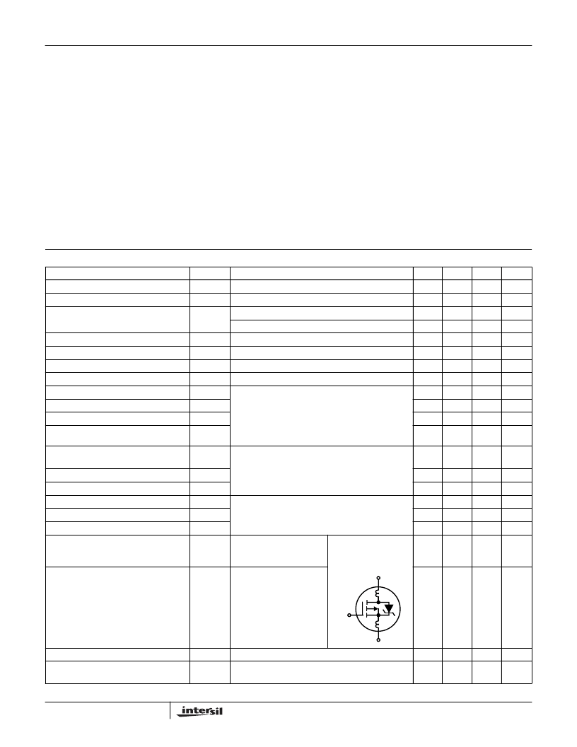
Internal Drain Inductance
Measured From the Drain
Lead, 5mm (0.2in) From
Package to Center of Die
Modified MOSFET
Symbol Showing the In-
ternal Devices
Inductances
-
5.0
-
nH
Internal Source Inductance
L
S
Measured From the Source
Lead, 5mm (0.2in) From
Header to Source Bonding
Pad
-
15
-
nH
Thermal Resistance Junction to Case
R
θ
JC
R
θ
JA
-
-
5.0
o
C/W
o
C/W
Thermal Resistance
Junction to Ambient
Typical Socket Mount
-
-
175
L
S
L
D
G
D
S
IRFF9230
相关PDF资料 |
PDF描述 |
|---|---|
| IRFG110 | POWER MOSFET THRU-HOLE (MO-036AB) |
| IRFG5110 | 100V, Combination 2N-2P-CHANNEL |
| IRFG6110 | POWER MOSFET THRU-HOLE (MO-036AB) |
| IRFG9110 | POWER MOSFET THRU-HOLE (MO-036AB) |
| IRFI4905 | HEXFET Power MOSFET |
相关代理商/技术参数 |
参数描述 |
|---|---|
| IRFF9231 | 制造商:International Rectifier 功能描述: |
| IRFF9232 | 制造商:Harris Corporation 功能描述: 制造商:International Rectifier 功能描述: |
| IRFF9233 | 制造商:International Rectifier 功能描述: |
| IRFG110 | 制造商:International Rectifier 功能描述:Trans MOSFET N-CH 100V 1A 14-Pin MO-036AB 制造商:International Rectifier 功能描述:TRANS MOSFET N-CH 100V 1A 14PIN MO-036AB - Bulk 制造商:International Rectifier 功能描述:Single N-Channel 100 V 1.4 W 15 nC Hexfet Power Mosfet Through Hole - MO-036AB 制造商:International Rectifier 功能描述:N CHANNEL MOSFET, 100V, MO-036AB; Transistor Polarity:N Channel; Continuous Drain Current Id:1A; Drain Source Voltage Vds:100V; On Resistance Rds(on):700mohm; Rds(on) Test Voltage Vgs:10V; Threshold Voltage Vgs Typ:4V; No. of Pins:14;RoHS Compliant: No |
| IRFG5110 | 制造商:International Rectifier 功能描述:TRANS MOSFET N/P-CH 100V 1A 14PIN MO-036AB - Bulk |
发布紧急采购,3分钟左右您将得到回复。