- 您现在的位置:买卖IC网 > PDF目录378639 > IRFI630B (FAIRCHILD SEMICONDUCTOR CORP) 200V N-Channel MOSFET PDF资料下载
参数资料
| 型号: | IRFI630B |
| 厂商: | FAIRCHILD SEMICONDUCTOR CORP |
| 元件分类: | JFETs |
| 英文描述: | 200V N-Channel MOSFET |
| 中文描述: | 9 A, 200 V, 0.4 ohm, N-CHANNEL, Si, POWER, MOSFET |
| 封装: | I2PAK-3 |
| 文件页数: | 1/9页 |
| 文件大小: | 648K |
| 代理商: | IRFI630B |
2002 Fairchild Semiconductor Corporation
Rev. C, December 2002
I
IRFW630B / IRFI630B
200V N-Channel MOSFET
General Description
These N-Channel enhancement mode power field effect
transistors are produced using Fairchild’s proprietary,
planar, DMOS technology.
This advanced technology has been especially tailored to
minimize on-state resistance, provide superior switching
performance, and withstand high energy pulse in the
avalanche and commutation mode. These devices are well
suited for high efficiency switching DC/DC converters,
switch mode power supplies, DC-AC converters for
uninterrupted power supply and motor control.
Features
9.0A, 200V, R
DS(on)
= 0.4
@V
GS
= 10 V
Low gate charge ( typical 22 nC)
Low Crss ( typical 22 pF)
Fast switching
100% avalanche tested
Improved dv/dt capability
Absolute Maximum Ratings
T
C
= 25°C unless otherwise noted
Thermal Characteristics
Symbol
V
DSS
I
D
Parameter
IRFW630B / IRFI630B
200
9.0
5.7
36
±
30
160
9.0
7.2
5.5
3.13
72
0.57
-55 to +150
Units
V
A
A
A
V
mJ
A
mJ
V/ns
W
W
W/°C
°C
Drain-Source Voltage
Drain Current
- Continuous (T
C
= 25°C)
- Continuous (T
C
= 100°C)
- Pulsed
I
DM
V
GSS
E
AS
I
AR
E
AR
dv/dt
P
D
Drain Current
Gate-Source Voltage
Single Pulsed Avalanche Energy
Avalanche Current
Repetitive Avalanche Energy
Peak Diode Recovery dv/dt
Power Dissipation (T
A
= 25°C) *
Power Dissipation (T
C
= 25°C)
(Note 1)
(Note 2)
(Note 1)
(Note 1)
(Note 3)
- Derate above 25°C
T
J
, T
stg
Operating and Storage Temperature Range
Maximum lead temperature for soldering purposes,
1/8
"
from case for 5 seconds
T
L
300
°C
Symbol
R
θ
JC
R
θ
JA
R
θ
JA
* When mounted on the minimum pad size recommended (PCB Mount)
Parameter
Typ
--
--
--
Max
1.74
40
62.5
Units
°C
/
W
°C
/
W
°C
/
W
Thermal Resistance, Junction-to-Case
Thermal Resistance, Junction-to-Ambient *
Thermal Resistance, Junction-to-Ambient
●
●
●
●
●
▲
!
S
!
!
!
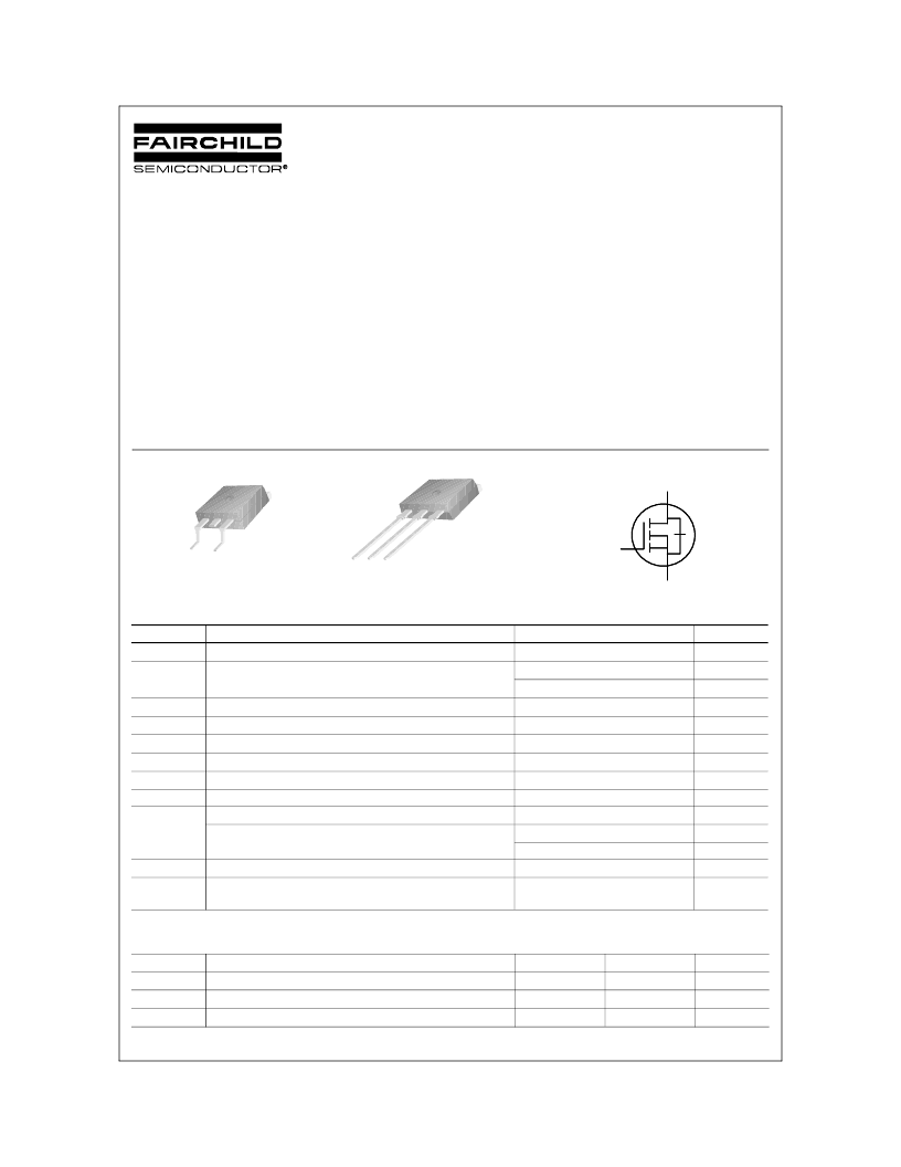
D
G
D
2
-PAK
IRFW Series
I
2
-PAK
IRFI Series
G
S
D
G
S
D
相关PDF资料 |
PDF描述 |
|---|---|
| IRFW634B | 250V N-Channel MOSFET |
| IRFI634 | 250V N-Channel MOSFET |
| IRFI634B | 250V N-Channel MOSFET |
| IRFW720S | N-Channel Power MOSFET(400V,1.8Ω,3.3A)(N沟道功率MOS场效应管(漏源电压400V,导通电阻1.8Ω,漏电流3.3A)) |
| IRFW740S | 400V N-Channel Power MOSFET(漏源电压为400V的N沟道增强型功率MOS场效应管) |
相关代理商/技术参数 |
参数描述 |
|---|---|
| IRFI630BTLTU_FP001 | 功能描述:MOSFET RoHS:否 制造商:STMicroelectronics 晶体管极性:N-Channel 汲极/源极击穿电压:650 V 闸/源击穿电压:25 V 漏极连续电流:130 A 电阻汲极/源极 RDS(导通):0.014 Ohms 配置:Single 最大工作温度: 安装风格:Through Hole 封装 / 箱体:Max247 封装:Tube |
| IRFI630BTU | 制造商:Rochester Electronics LLC 功能描述: 制造商:Fairchild Semiconductor Corporation 功能描述: |
| IRFI630BTU_FP001 | 功能描述:MOSFET 200V N-Ch B-FET RoHS:否 制造商:STMicroelectronics 晶体管极性:N-Channel 汲极/源极击穿电压:650 V 闸/源击穿电压:25 V 漏极连续电流:130 A 电阻汲极/源极 RDS(导通):0.014 Ohms 配置:Single 最大工作温度: 安装风格:Through Hole 封装 / 箱体:Max247 封装:Tube |
| IRFI630G | 功能描述:MOSFET N-Chan 200V 5.9 Amp RoHS:否 制造商:STMicroelectronics 晶体管极性:N-Channel 汲极/源极击穿电压:650 V 闸/源击穿电压:25 V 漏极连续电流:130 A 电阻汲极/源极 RDS(导通):0.014 Ohms 配置:Single 最大工作温度: 安装风格:Through Hole 封装 / 箱体:Max247 封装:Tube |
| IRFI630GPBF | 功能描述:MOSFET N-Chan 200V 5.9 Amp RoHS:否 制造商:STMicroelectronics 晶体管极性:N-Channel 汲极/源极击穿电压:650 V 闸/源击穿电压:25 V 漏极连续电流:130 A 电阻汲极/源极 RDS(导通):0.014 Ohms 配置:Single 最大工作温度: 安装风格:Through Hole 封装 / 箱体:Max247 封装:Tube |
发布紧急采购,3分钟左右您将得到回复。