- 您现在的位置:买卖IC网 > PDF目录377522 > IRHN7250 (International Rectifier) HEXFET Transistor(HEXFET 晶体管) PDF资料下载
参数资料
| 型号: | IRHN7250 |
| 厂商: | International Rectifier |
| 英文描述: | HEXFET Transistor(HEXFET 晶体管) |
| 中文描述: | 的HEXFET晶体管(之HEXFET晶体管) |
| 文件页数: | 2/12页 |
| 文件大小: | 274K |
| 代理商: | IRHN7250 |
IRHN7250, IRHN8250, JANSR-, JANSH-, 2N7269U
Devices
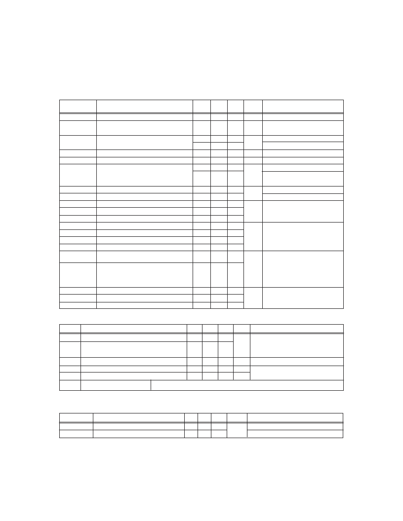
Electrical Characteristics
@ Tj = 25°C (Unless Otherwise Specified)
2
www.irf.com
Parameter
Drain-to-Source Breakdown Voltage
BVDSS/
TJ Temperature Coefficient of Breakdown
Voltage
RDS(on)
Static Drain-to-Source On-State
Resistance
VGS(th)
Gate Threshold Voltage
gfs
Forward Transconductance
IDSS
Zero Gate Voltage Drain Current
Min
200
—
Typ
—
0.27
Max Units
—
—
Test Conditions
VGS = 0V, ID = 1.0mA
Reference to 25°C, ID = 1.0mA
BVDSS
V
V/°C
—
—
2.0
8.0
—
—
—
— 0.11
—
4.0
V
VDS = VGS, ID = 1.0mA
—
—
S (
)
VDS > 15V, IDS = 16A
—
25
VDS= 0.8 x Max Rating,VGS=0V
—
250
VDS = 0.8 x Max Rating
VGS = 0V, TJ = 125°C
—
100
—
-100
—
170
—
30
nC
VDS = Max Rating x 0.5
—
60
—
33
VDD = 100V, ID = 26A,
—
140
—
140
—
140
2.0
—
nH
0.10
VGS = 12V, ID = 16A
IGSS
IGSS
Qg
Qgs
Qgd
td
(on)
tr
td
(off)
tf
LD
Gate-to-Source Leakage Forward
Gate-to-Source Leakage Reverse
Total Gate Charge
Gate-to-Source Charge
Gate-to-Drain (‘Miller’) Charge
Turn-On Delay Time
Rise Time
Turn-Off Delay Time
Fall Time
Internal Drain Inductance
—
—
—
—
—
—
—
—
—
—
VGS = 20V
VGS = -20V
VGS =12V, ID = 26A
RG = 2.35
LS
Internal Source Inductance
—
4.1
—
Ciss
Coss
Crss
Input Capacitance
Output Capacitance
Reverse Transfer Capacitance
—
—
—
4700
850
210
—
—
—
VGS = 0V, VDS = 25V
f = 1.0MHz
pF
nA
ns
μ
A
Source-Drain Diode Ratings and Characteristics
Parameter
IS
Continuous Source Current (Body Diode)
ISM
Pulse Source Current (Body Diode)
Min Typ
—
—
Max Units
26
104
Test Conditions
—
—
VSD
trr
QRR
ton
Diode Forward Voltage
Reverse Recovery Time
Reverse Recovery Charge
—
—
—
—
—
—
1.4
820
12
V
ns
μ
C
T
j
= 25°C, IS = 26A, VGS = 0V
Tj = 25°C, IF = 26A, di/dt
≥
100A/
μ
s
VDD
≤
25V
Forward Turn-On Time
Intrinsic turn-on time is negligible. Turn-on speed is substantially controlled by LS + LD.
A
Thermal Resistance
Parameter
RthJC
Junction-to-Case
RthJ-PCB
Junction-to-PC board
Min Typ Max
—
—
—
6.6
Units
Test Conditions
0.83
— Soldered to a 1 inch square clad PC board
°C/W
Pre-Irradiation
相关PDF资料 |
PDF描述 |
|---|---|
| IRHN8250 | HEXFET Transistor(HEXFET 晶体管) |
| IRHN9130 | P-Channel,-100 Volt, 0.3Ω, RAD HARD HEXFET(P沟道,-100 V, 0.3Ω,抗辐射HEXFET晶体管) |
| IRHN93130 | P-Channel,-100 Volt, 0.3Ω, RAD HARD HEXFET(P沟道,-100 V, 0.3Ω,抗辐射HEXFET晶体管) |
| IRHN9230 | P-Channel RAD HARD HEXFET TRANSISTOR(P 沟道 Rad Hard 技术 HEXFET晶体管) |
| IRHN9250 | HEXFET Transistor(HEXFET 晶体管) |
相关代理商/技术参数 |
参数描述 |
|---|---|
| IRHN7250SE | 制造商:International Rectifier 功能描述:HIREL, HEXFET RHD - Bulk |
| IRHN7250SESCS | 制造商:International Rectifier 功能描述:HIREL, HEXFET RHD - Bulk |
| IRHN7450 | 制造商:International Rectifier 功能描述:HEXFET, HIREL, RAD HARD,G4 - Bulk |
| IRHN7450SCS | 制造商:International Rectifier 功能描述:HIREL, HEXFET RHD - Bulk |
| IRHN7450SE | 制造商:International Rectifier 功能描述:HEXFET, HIREL, RAD HARD,G4 - Bulk |
发布紧急采购,3分钟左右您将得到回复。