- 您现在的位置:买卖IC网 > PDF目录17638 > IRLR8503PBF (International Rectifier)MOSFET N-CH 30V 44A DPAK PDF资料下载
参数资料
| 型号: | IRLR8503PBF |
| 厂商: | International Rectifier |
| 文件页数: | 3/9页 |
| 文件大小: | 0K |
| 描述: | MOSFET N-CH 30V 44A DPAK |
| 标准包装: | 75 |
| 系列: | HEXFET® |
| FET 型: | MOSFET N 通道,金属氧化物 |
| FET 特点: | 逻辑电平门 |
| 漏极至源极电压(Vdss): | 30V |
| 电流 - 连续漏极(Id) @ 25° C: | 44A |
| 开态Rds(最大)@ Id, Vgs @ 25° C: | 16 毫欧 @ 15A,10V |
| Id 时的 Vgs(th)(最大): | 3V @ 250µA |
| 闸电荷(Qg) @ Vgs: | 20nC @ 5V |
| 输入电容 (Ciss) @ Vds: | 1650pF @ 25V |
| 功率 - 最大: | 62W |
| 安装类型: | 表面贴装 |
| 封装/外壳: | TO-252-3,DPak(2 引线+接片),SC-63 |
| 供应商设备封装: | D-Pak |
| 包装: | 管件 |
�� �
�
�IRLR8503PbF�
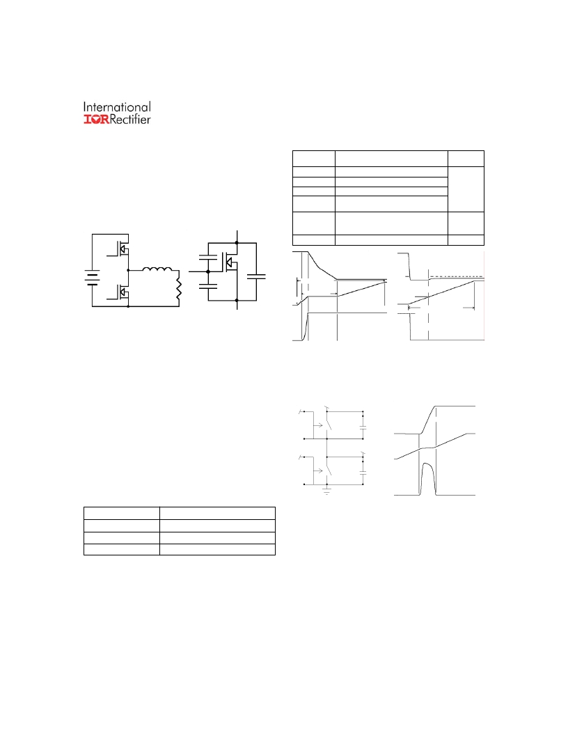
�Power� MOSFET� Optimization� for� DC-DC� Converters�
�While� the� IRLR8103V� and� IRLR8503� can� and� are� be-�
�Table� 2� –� New� Charge� Parameters�
�ing� used� in� a� variety� of� applications,� they� were� designed�
�and� optimized� for� low� voltage� DC-DC� conversion� in� a�
�synchronous� buck� converter� topology,� specifically,� mi-�
�croprocessor� power� applications.� The� IRLR8503� (Fig-�
�ure� 1)� was� optimized� for� the� control� FET� socket,� while�
�the� IRLR8103V� was� optimized� for� the� synchronous�
�FET� function.�
�New� Charge�
�Parameter�
�Q� GS1�
�Q� GS2�
�Q� GCONT�
�Q� SWITCH�
�Q� OSS�
�Description�
�Pre-Threshold� Gate� Charge�
�Post-Threshold� Gate� Charge�
�Control� FET� Total� Q� G�
�Charge� during� control� FET� switching�
�Combines� Q� GS2� and� Q� GD�
�Output� charge�
�Charge� supplied� to� C� OSS� during� the� Q� GD�
�period� of� control� FET� switching�
�Waveform�
�Figure� 3�
�Figure� 5�
�Figure� 6�
�I� RLR8503�
�(Cont� FET)�
�CGD�
�Q� GSYNC�
�Synchronous� FET� Total� Q� G� (V� DS� ≤� 0)� Figure� 4�
�Drain� Voltage�
�Drain� Voltage�
�IRLR8103V�
�(Sync� FET)�
�CGS�
�CDS�
�VGTH�
�QG�
�(Control� FET)�
�QSwitch�
�QGD�
�Gate� Voltage�
�Dead�
�0V� Time�
�Gate� Voltage�
�VGTH�
�Figure� 1� –� Application�
�Figure� 2� –� Inter-electrode�
�QG� (Sync� FET)�
�0A�
�Drain� Current�
�Topology� Capacitance�
�Because� of� the� inter-electrode� capacitance� (Figure� 2)�
�of� the� Power� MOSFET,� specifying� the� R� DSON� of� the� de-�
�vice� is� not� enough� to� ensure� good� performance.� An�
�Drain� Current�
�Figure� 3� –� Control� FET�
�Waveform�
�Body�
�Diode�
�Current�
�Figure� 4� –� Sync� FET�
�Waveform�
�optimization� between� R� DSON� and� charge� must� be� per-�
�formed� to� insure� the� best� performing� MOSFET� for� a�
�given� application.� Both� die� size� and� device� architec-�
�The� waveforms� are� broken� into� segments� correspond-�
�ing� to� charge� parameters.� These,� in� turn,� correspond�
�to� discrete� time� segments� of� the� switching� waveform.�
�ture� must� be� varied� to� achieve� the� minimum� possible�
�in-circuit� losses.� This� is� independently� true� for� both�
�control� FET� and� synchronous� FET.� Unfortunately,� the�
�capacitances� of� a� FET� are� non-linear� and� voltage� de-�
�pendent.� Therefore,� it� is� inconvenient� to� specify� and�
�use� them� effectively� in� switching� power� supply� power�
�loss� estimations.� This� was� well� understood� years� ago�
�and� resulted� in� changing� the� emphasis� from� capaci-�
�tance� to� gate� charge� on� Power� MOSFET� data� sheets.�
�g1�
�g2�
�VIN�
�N1�
�Cont� FET�
�N2�
�Sync� FET�
�Coss1�
�2n�
�SN�
�Coss2�
�2n�
�Switch� node� voltage�
�(VSN)�
�N1� Gate�
�Voltage�
�N1� Current�
�N1� Coss� Discharge�
�+�
�N2� Coss� Charge�
�Table� 1� –� Traditional� Charge� Parameters�
�Device� Capacitance� Corresponding� Charge� Parameter�
�Figure� 5� –� Q� OSS�
�Equivalent� Circuit�
�Figure� 6� –� Q� OSS�
�Waveforms�
�C� GS�
�C� GS� +� C� GD�
�C� GD�
�Q� GS�
�Q� G�
�Q� GD�
�Losses� may� be� broken� into� four� categories:� conduc-�
�tion� loss,� gate� drive� loss,� switching� loss,� and� output�
�loss.� The� following� simplified� power� loss� equation� is�
�International� Rectifier� has� recently� taken� the� industry�
�a� step� further� by� specifying� new� charge� parameters�
�that� are� even� more� specific� to� DC-DC� converter� de-�
�sign� (Table� 2).� In� order� to� understand� these� parameters,�
�it� is� best� to� start� with� the� in-circuit� waveforms� in� Fig-�
�ure� 3� &� Figure� 4.�
�www.irf.com�
�true� for� both� MOSFETs� in� a� synchronous� buck� con-�
�verter:�
�P� LOSS� =� P� CONDUCTION� +� P� GATE� DRIVE� +� P� SWITCH� +� P� OUTPUT�
�For� the� synchronous� FET,� the� P� SWITCH� term� becomes�
�virtually� zero� and� is� ignored.�
�3�
�相关PDF资料 |
PDF描述 |
|---|---|
| R1D10-1515/P | CONV DC/DC 1W 15VIN +/-15VOUT |
| TC4422AVMF713 | IC MOSFET DRVR 9A N-INV 8DFN |
| R1D10-1512/P | CONV DC/DC 1W 15VIN +/-12VOUT |
| TC4421AVMF713 | IC MOSFET DRIVER 9A INV 8DFN |
| 3266X-1-100LF | TRIMMER 10 OHM 0.25W TH |
相关代理商/技术参数 |
参数描述 |
|---|---|
| IRLR8503TR | 功能描述:MOSFET N-CH 30V 44A DPAK RoHS:否 类别:分离式半导体产品 >> FET - 单 系列:HEXFET® 标准包装:1,000 系列:MESH OVERLAY™ FET 型:MOSFET N 通道,金属氧化物 FET 特点:逻辑电平门 漏极至源极电压(Vdss):200V 电流 - 连续漏极(Id) @ 25° C:18A 开态Rds(最大)@ Id, Vgs @ 25° C:180 毫欧 @ 9A,10V Id 时的 Vgs(th)(最大):4V @ 250µA 闸电荷(Qg) @ Vgs:72nC @ 10V 输入电容 (Ciss) @ Vds:1560pF @ 25V 功率 - 最大:40W 安装类型:通孔 封装/外壳:TO-220-3 整包 供应商设备封装:TO-220FP 包装:管件 |
| IRLR8503TRHR | 制造商:International Rectifier 功能描述:Trans MOSFET N-CH 30V 44A 3-Pin(2+Tab) DPAK T/R |
| IRLR8503TRL | 功能描述:MOSFET N-CH 30V 44A DPAK RoHS:否 类别:分离式半导体产品 >> FET - 单 系列:HEXFET® 标准包装:1,000 系列:MESH OVERLAY™ FET 型:MOSFET N 通道,金属氧化物 FET 特点:逻辑电平门 漏极至源极电压(Vdss):200V 电流 - 连续漏极(Id) @ 25° C:18A 开态Rds(最大)@ Id, Vgs @ 25° C:180 毫欧 @ 9A,10V Id 时的 Vgs(th)(最大):4V @ 250µA 闸电荷(Qg) @ Vgs:72nC @ 10V 输入电容 (Ciss) @ Vds:1560pF @ 25V 功率 - 最大:40W 安装类型:通孔 封装/外壳:TO-220-3 整包 供应商设备封装:TO-220FP 包装:管件 |
| IRLR8503TRLPBF | 功能描述:MOSFET N-CH 30V 44A DPAK RoHS:是 类别:分离式半导体产品 >> FET - 单 系列:HEXFET® 标准包装:1,000 系列:MESH OVERLAY™ FET 型:MOSFET N 通道,金属氧化物 FET 特点:逻辑电平门 漏极至源极电压(Vdss):200V 电流 - 连续漏极(Id) @ 25° C:18A 开态Rds(最大)@ Id, Vgs @ 25° C:180 毫欧 @ 9A,10V Id 时的 Vgs(th)(最大):4V @ 250µA 闸电荷(Qg) @ Vgs:72nC @ 10V 输入电容 (Ciss) @ Vds:1560pF @ 25V 功率 - 最大:40W 安装类型:通孔 封装/外壳:TO-220-3 整包 供应商设备封装:TO-220FP 包装:管件 |
| IRLR8503TRPBF | 功能描述:MOSFET N-CH 30V 44A DPAK RoHS:是 类别:分离式半导体产品 >> FET - 单 系列:HEXFET® 标准包装:1,000 系列:MESH OVERLAY™ FET 型:MOSFET N 通道,金属氧化物 FET 特点:逻辑电平门 漏极至源极电压(Vdss):200V 电流 - 连续漏极(Id) @ 25° C:18A 开态Rds(最大)@ Id, Vgs @ 25° C:180 毫欧 @ 9A,10V Id 时的 Vgs(th)(最大):4V @ 250µA 闸电荷(Qg) @ Vgs:72nC @ 10V 输入电容 (Ciss) @ Vds:1560pF @ 25V 功率 - 最大:40W 安装类型:通孔 封装/外壳:TO-220-3 整包 供应商设备封装:TO-220FP 包装:管件 |
发布紧急采购,3分钟左右您将得到回复。