- 您现在的位置:买卖IC网 > PDF目录11818 > IS82C50A-5 (Intersil)IC PERIPH UART/BRG 10MHZ 44-PLCC PDF资料下载
参数资料
| 型号: | IS82C50A-5 |
| 厂商: | Intersil |
| 文件页数: | 20/25页 |
| 文件大小: | 0K |
| 描述: | IC PERIPH UART/BRG 10MHZ 44-PLCC |
| 标准包装: | 26 |
| 特点: | 单芯片 UART/BRG |
| 通道数: | 1,UART |
| 规程: | RS232C |
| 电源电压: | 4.5 V ~ 5.5 V |
| 带并行端口: | 是 |
| 带故障启动位检测功能: | 是 |
| 带调制解调器控制功能: | 是 |
| 带CMOS: | 是 |
| 安装类型: | 表面贴装 |
| 封装/外壳: | 44-LCC(J 形引线) |
| 供应商设备封装: | 44-PLCC |
| 包装: | 管件 |
4
FN2958.5
August 24, 2006
82C50A
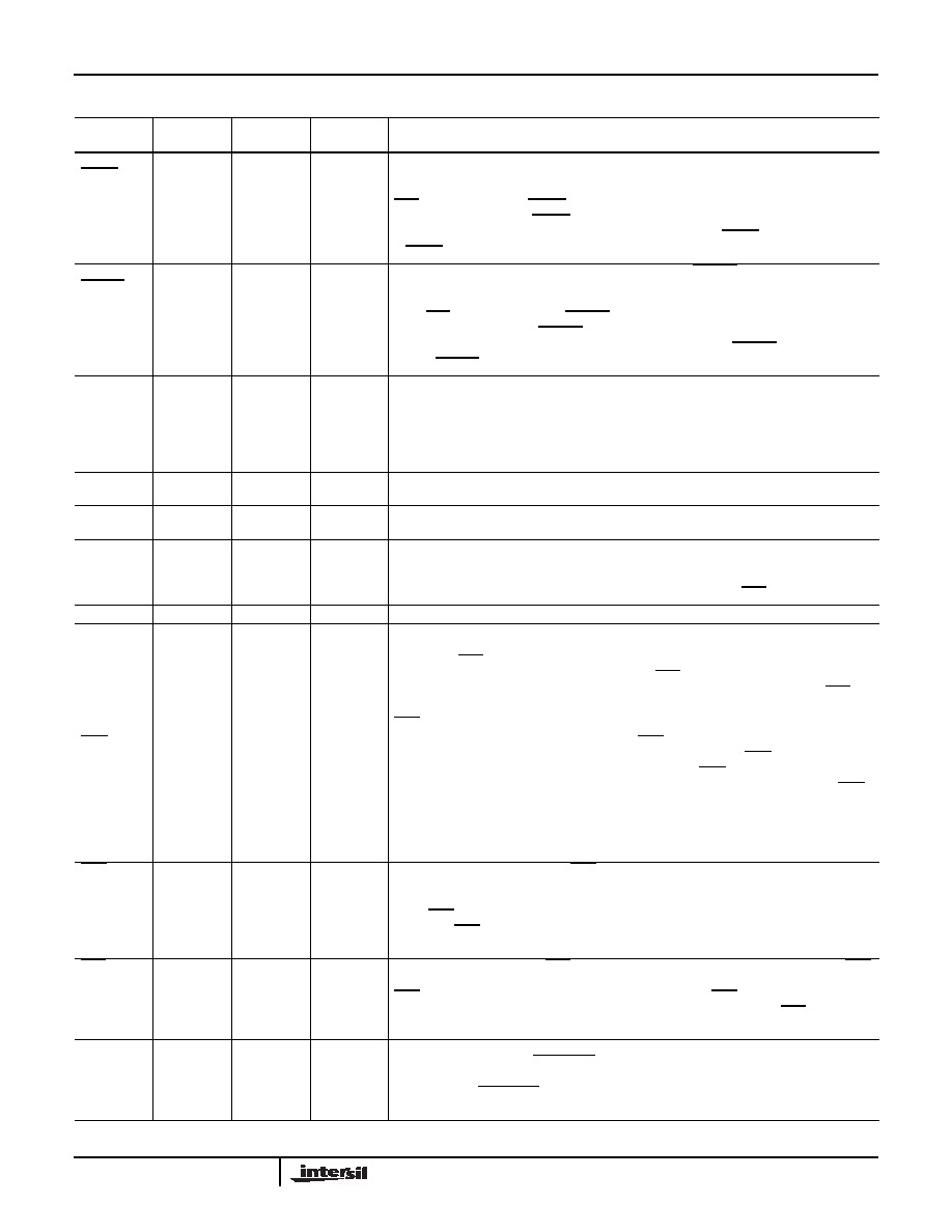
Pin Description
SYMBOL
PIN
NUMBER
TYPE
ACTIVE
LEVEL
DESCRIPTION
DISTR,
DISTR
22
21
I
H
L
DATA IN STROBE, DATA IN STROBE: DISTR, DISTR are read inputs which cause the
82C50A to output data to the data bus (D0-D7). The data output depends upon the
register selected by the address inputs A0, A1, A2. The chip select inputs CS0, CS1,
CS2 enable the DISTR, DISTR inputs.
Only an active DISTR or DISTR, not both, is used to receive data from the 82C50A
during a read operation. If DISTR is used as the read input, DlSTR should be tied high.
If DISTR is used as the active read input, DISTR should be tied low.
DOSTR,
DOSTR
19
18
I
H
L
DATA OUT STROBE, DATA OUT STROBE: DOSTR, DOSTR are write inputs which
cause data from the data bus (D0-D7) to be input to the 82C50A. The data input depends
upon the register selected by the address inputs A0, A1, A2. The chip select inputs CS0,
CS1, CS2 enable the DOSTR, DOSTR inputs.
Only an active DOSTR or DOSTR, not both, is used to transmit data to the 82C50A
during a write operation. If DOSTR is used as the write input, DOSTR should be tied
high. If DOSTR is used as the write input, DOSTR should be tied low.
D0-D7
1-8
I/O
DATA BITS 0-7: The Data Bus provides eight, three-state input/output lines for the
transfer of data, control and status information between the 82C50A and the CPU. For
character formats of less than 8 bits, D7, D6 and D5 are “don’t cares” for data write
operations and 0 for data read operations. These lines are normally in a high impedance
state except during read operations. D0 is the Least Significant Bit (LSB) and is the first
serial data bit to be received or transmitted.
A0, A1,
A2
28, 27,
26
I
H
REGISTER SELECT: The address lines select the internal registers during CPU bus
operations. See Table 1.
XTAL1,
XTAL2
16
17
I
O
CRYSTAL/CLOCK: Crystal connections for the internal Baud Rate Generator. XTAL1
can also be used as an external clock input, in which case XTAL2 should be left open.
SOUT
11
O
SERIAL DATA OUTPUT: Serial data output from the 82C50A transmitter circuitry. A
Mark (1) is a logic one (high) and Space (0) is a logic zero (low). SOUT is held in the
Mark condition when the transmitter is disabled, MR is true, the Transmitter Register is
empty, or when in the Loop Mode. SOUT is not affected by the CTS input.
GND
20
L
GROUND: Power supply ground connection (VSS).
CTS
36
I
L
CLEAR TO SEND: The logical state of the CTS pin is reflected in the CTS bit of the
(MSR) Modem Status Register (CTS is bit 4 of the MSR, written MSR (4)). A change of
state in the CTS pin since the previous reading of the MSR causes the setting of DCTS
(MSR(O)) of the Modem Status Register. When CTS pin is ACTIVE (low), the modem is
indicating that data on SOUT can be transmitted on the communications link. If CTS pin
goes INACTIVE (high), the 82C50A should not be allowed to transmit data out of SOUT.
CTS pin does not affect Loop Mode operation.
DSR
37
I
L
DATA SET READY: The logical state of the DSR pin is reflected in MSR(5) of the
Modem Status Register. DDSR (MSR(1)) indicates whether the DSR pin has changed
state since the previous reading of the MSR. When the DSR pin is ACTIVE (low), the
modem is indicating that it is ready to exchange data with the 82C50A, while the DSR
Pin INACTIVE (high) indicates that the modem is not ready for data exchange. The
ACTIVE condition indicates only the condition of the local Data Communications
Equipment (DCE), and does not imply that a data circuit as been established with remote
equipment.
DTR
33
O
L
DATA TERMINAL READY: The DTR pin can be set (low) by writing a logic 1 to MCR(0),
Modem Control Register bit 0. This signal is cleared (high) by writing a logic 0 to the DTR
bit (MCR(0)) or whenever a MR ACTIVE (high) is applied to the 82C50A. When ACTIVE
(low), DTR pin indicates to the DCE that the 82C50A is ready to receive data. In some
instances, DTR pin is used as a power on indicator. The INACTIVE (high) state causes
the DCE to disconnect the modem from the telecommunications circuit.
RTS
32
O
L
REQUEST TO SEND: The RTS signal is an output used to enable the modem. The RTS
pin is set low by writing a logic 1 to MCR (1) bit 1 of the Modem Control Register. The
RTS pin is reset high by Master Reset. When ACTIVE, the RTS pin indicates to the DCE
that the 82C50A has data ready to transmit. In half duplex operations, RTS is used to
control the direction of the line.
BAUDOUT
15
O
BAUDOUT: This output is a 16X clock out used for the transmitter section (16X = 16
times the data rate). The BAUDOUT clock rate is equal to the reference oscillator
frequency divided by the specified divisor in the Baud Rate Generator Divisor Latches
DLL and DLM. BAUDOUT may be used by the Receiver section by tying this output to
RCLK.
相关PDF资料 |
PDF描述 |
|---|---|
| IS82C50A-5Z | IC PERIPH UART/BRG 10MHZ 44-PLCC |
| ATMEGA329-16MUR | MCU AVR 32K FLASH 16MHZ 64QFN |
| CS82C50A-5Z96 | IC ASYNC COMM ELEMNT UART 44PLCC |
| CS82C50A-5Z | IC COMMUNICATION ELEMENT 44-PLCC |
| CP82C52Z | IC UART/BRG 5V 16MHZ 28-PDIP |
相关代理商/技术参数 |
参数描述 |
|---|---|
| IS82C50A-5Z | 功能描述:UART 接口集成电路 W/ANNEAL PERIPH UART /BRG 5V 10MHZ RoHS:否 制造商:Texas Instruments 通道数量:2 数据速率:3 Mbps 电源电压-最大:3.6 V 电源电压-最小:2.7 V 电源电流:20 mA 最大工作温度:+ 85 C 最小工作温度:- 40 C 封装 / 箱体:LQFP-48 封装:Reel |
| IS82C52 | 功能描述:UART 接口集成电路 PERIPH UART/BRG 5V 16MHZ 28PLCC IND RoHS:否 制造商:Texas Instruments 通道数量:2 数据速率:3 Mbps 电源电压-最大:3.6 V 电源电压-最小:2.7 V 电源电流:20 mA 最大工作温度:+ 85 C 最小工作温度:- 40 C 封装 / 箱体:LQFP-48 封装:Reel |
| IS82C52/TR100/BAE | 制造商:Intersil Corporation 功能描述:PERIPH UART/BRG 5V 16MHZ 28PLCC IND - Tape and Reel |
| IS82C5296 | 制造商:Rochester Electronics LLC 功能描述:- Bulk |
| IS82C52R2490 | 制造商:Rochester Electronics LLC 功能描述:- Bulk |
发布紧急采购,3分钟左右您将得到回复。