参数资料
| 型号: | ISL12028IVAZ |
| 厂商: | Intersil |
| 文件页数: | 6/29页 |
| 文件大小: | 0K |
| 描述: | IC RTC/CALENDAR EEPROM 14-TSSOP |
| 产品培训模块: | Solutions for Industrial Control Applications |
| 标准包装: | 960 |
| 类型: | 时钟/日历 |
| 特点: | 警报器,闰年,监控器,监视计时器 |
| 时间格式: | HH:MM:SS(12/24 小时) |
| 数据格式: | YY-MM-DD-dd |
| 接口: | I²C,2 线串口 |
| 电源电压: | 2.7 V ~ 5.5 V |
| 电压 - 电源,电池: | 1.8 V ~ 5.5 V |
| 工作温度: | -40°C ~ 85°C |
| 安装类型: | 表面贴装 |
| 封装/外壳: | 14-TSSOP(0.173",4.40mm 宽) |
| 供应商设备封装: | 14-TSSOP |
| 包装: | 管件 |
第1页第2页第3页第4页第5页当前第6页第7页第8页第9页第10页第11页第12页第13页第14页第15页第16页第17页第18页第19页第20页第21页第22页第23页第24页第25页第26页第27页第28页第29页
14
FN8233.9
November 30, 2010
The effective series load capacitance is the combination of
For example, CLOAD(ATR = 00000) = 12.5pF, CLOAD
(ATR = 100000) = 4.5pF, and CLOAD(ATR = 011111) = 20.25pF.
The entire range for the series combination of load capacitance
goes from 4.5pF to 20.25pF in 0.25pF steps. Note that these
are typical values.
DTR Register - DTR2, DTR1, DTR0: Digital
Trimming Register
The digital trimming Bits DTR2, DTR1 and DTR0 adjust the
number of counts per second and average the ppm error to
achieve better accuracy.
DTR2 is a sign bit. DTR2 = 0 means frequency
compensation is > 0. DTR2 = 1 means frequency
compensation is < 0.
DTR1 and DTR0 are scale bits. DTR1 gives 10ppm
adjustment and DTR0 gives 20ppm adjustment.
A range from -30ppm to +30ppm can be represented by
using the three DTR bits.
PWR Register: SBIB, BSW, VTS2, VTS1, VTS0
SBIB: - Serial Bus Interface (Enable)
The serial bus can be disabled in battery backup mode by
setting this bit to “1”. This will minimize power drain on the
battery. The Serial Interface can be enabled in battery
backup mode by setting this bit to “0”. (default is “0”). See
BSW: Power Control Bit
The Power Control bit, BSW, determines the conditions for
switching between VDD and Back Up Battery. There are two
options.
Option 1 Standard Mode: Set “BSW = 0” (default for
ISL12028A)
Option 2 Legacy/Default Mode: Set “BSW = 1” (default for
ISL12028)
See “Power Control Operation” on page 15 for more details.
Also see “I2C Communications During Battery backup and
LVR Operation” in the “Application Section” on page 22 for
important details.
VTS2, VTS1, VTS0: VRESET Select Bits
The ISL12028 is shipped with a default VDD threshold
This register is a non-volatile with no protection, therefore
any writes to this location can change the default value from
that marked on the package. If not changed with a
non-volatile write, this value will not change over normal
operating and storage conditions. However, ISL12028 has
four (4) additional selectable levels to fit the customers
application. Levels are: 4.64V(default), 4.38V, 3.09V, 2.92V
and 2.63V. The VRESET selection is via 3 bits (VTS2, VTS1
and VTS0) (see Table 6).
Care should be taken when changing the VRESET select bits.
If the VRESET voltage selected is higher than VDD, then the
device will go into RESET and unless VDD is increased, the
device will no longer be able to communicate using the I2C.
In battery mode, the RESET signal output is asserted LOW
when the VDD voltage supply has dipped below the VRESET
threshold, but the RESET signal output will not return HIGH
until the device is back to VDD mode even the VDD voltage is
above VRESET threshold.
Device Operation
Writing to the Clock/Control Registers
Changing any of the bits of the clock/control registers
requires the following steps:
1. Write a 02h to the Status Register to set the Write Enable
Latch (WEL). This is a volatile operation, so there is no
delay after the write. (Operation preceded by a start and
ended with a stop).
2. Write a 06h to the Status Register to set both the Register
Write Enable Latch (RWEL) and the WEL bit. This is also
a volatile cycle. The zeros in the data byte are required.
(Operation proceeded by a start and ended with a stop).
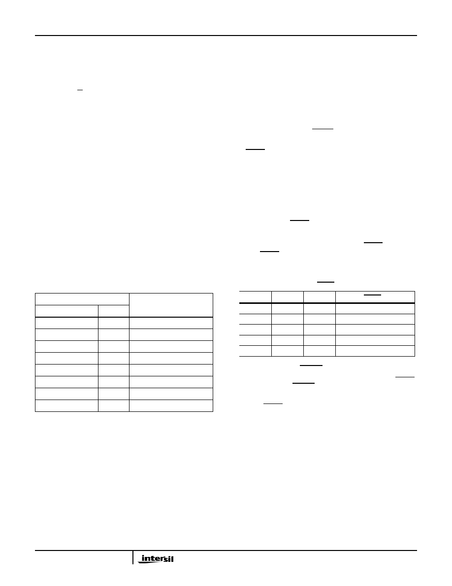
TABLE 5. DIGITAL TRIMMING REGISTERS
DTR REGISTER
ESTIMATED FREQUENCY
PPM
DTR2
DTR1
DTR0
00
0
01
0
+10
00
1
+20
01
1
+30
10
0
11
0
-10
10
1
-20
11
1
-30
C
LOAD
1
C
X1
-----------
1
C
X2
-----------
+
-----------------------------------
=
C
LOAD
16 b5
8 b4
4 b3
2 b2
1 b1
0.5 b0
9
+
+
+
+
+
+
2
-----------------------------------------------------------------------------------------------------------------------------
pF
=
(EQ. 2)
TABLE 6. VRESET SELECTION
VTS2
VTS1
VTS0
VRESET (V)
0
4.64
0
1
4.38
0
1
0
3.09
0
1
2.92
1
0
2.63
ISL12028, ISL12028A
相关PDF资料 |
PDF描述 |
|---|---|
| AD5206BN10 | IC DGTL POT 6CH 256POS 24-DIP |
| VI-2NT-MW | CONVERTER MOD DC/DC 6.5V 100W |
| VE-B3F-MY-F3 | CONVERTER MOD DC/DC 72V 50W |
| AD5280BRUZ200 | IC DGTL POT 200K 256POS 14-TSSOP |
| VE-B3F-MY-F2 | CONVERTER MOD DC/DC 72V 50W |
相关代理商/技术参数 |
参数描述 |
|---|---|
| ISL12028IVAZ-T | 功能描述:实时时钟 REAL TIME CLKRTC W/ EPROM 4 64VSET 14 RoHS:否 制造商:Microchip Technology 功能:Clock, Calendar. Alarm RTC 总线接口:I2C 日期格式:DW:DM:M:Y 时间格式:HH:MM:SS RTC 存储容量:64 B 电源电压-最大:5.5 V 电源电压-最小:1.8 V 最大工作温度:+ 85 C 最小工作温度: 安装风格:Through Hole 封装 / 箱体:PDIP-8 封装:Tube |
| ISL12028IVZ | 功能描述:实时时钟 REAL TIME CLKRTC W/ EPROM IN 14LD RoHS:否 制造商:Microchip Technology 功能:Clock, Calendar. Alarm RTC 总线接口:I2C 日期格式:DW:DM:M:Y 时间格式:HH:MM:SS RTC 存储容量:64 B 电源电压-最大:5.5 V 电源电压-最小:1.8 V 最大工作温度:+ 85 C 最小工作温度: 安装风格:Through Hole 封装 / 箱体:PDIP-8 封装:Tube |
| ISL12028IVZ-T | 功能描述:实时时钟 REAL TIME CLKRTC W/ EPROM IN 14LD T RoHS:否 制造商:Microchip Technology 功能:Clock, Calendar. Alarm RTC 总线接口:I2C 日期格式:DW:DM:M:Y 时间格式:HH:MM:SS RTC 存储容量:64 B 电源电压-最大:5.5 V 电源电压-最小:1.8 V 最大工作温度:+ 85 C 最小工作温度: 安装风格:Through Hole 封装 / 箱体:PDIP-8 封装:Tube |
| ISL12029 | 制造商:INTERSIL 制造商全称:Intersil Corporation 功能描述:Real Time Clock/Calendar with I2C Bus? and EEPROM |
| ISL12029_10 | 制造商:INTERSIL 制造商全称:Intersil Corporation 功能描述:Real Time Clock/Calendar with I2C Busa?¢ and EEPROM |
发布紧急采购,3分钟左右您将得到回复。