- 您现在的位置:买卖IC网 > PDF目录383128 > ISL1220 (Intersil Corporation) Low Power RTC with 8 Bytes of Battery Backed SRAM and Separate FOUT(具有电池供电的8位SRAM和独立输出的低功率RTC) PDF资料下载
参数资料
| 型号: | ISL1220 |
| 厂商: | Intersil Corporation |
| 英文描述: | Low Power RTC with 8 Bytes of Battery Backed SRAM and Separate FOUT(具有电池供电的8位SRAM和独立输出的低功率RTC) |
| 中文描述: | 低功耗RTC与8电池供电SRAM和独立的FOUT(具有电池供电的8位的SRAM和独立输出的低功率实时时钟字节) |
| 文件页数: | 16/20页 |
| 文件大小: | 328K |
| 代理商: | ISL1220 |
16
FN6315.0
June 22, 2006
Device Addressing
Following a start condition, the master must output a Slave
Address Byte. The 7 MSBs are the device identifier. These
bits are “1101111”. Slave bits “1101” access the register.
Slave bits “111” specify the device select bits.
The last bit of the Slave Address Byte defines a read or write
operation to be performed. When this R/W bit is a “1”, then a
read operation is selected. A “0” selects a write operation
(Refer to Figure 15).
After loading the entire Slave Address Byte from the SDA
bus, the ISL1220 compares the device identifier and device
select bits with “1101111”. Upon a correct compare, the
device outputs an acknowledge on the SDA line.
Following the Slave Byte is a one byte word address. The
word address is either supplied by the master device or
obtained from an internal counter. On power up the internal
address counter is set to address 0h, so a current address
read of the CCR array starts at address 0h. When required,
as part of a random read, the master must supply the 1 Word
Address Bytes as shown in Figure 16.
In a random read operation, the slave byte in the “dummy
write” portion must match the slave byte in the “read”
section. For a random read of the Clock/Control Registers,
the slave byte must be “1101111x” in both places.
Write Operation
A Write operation requires a START condition, followed by a
valid Identification Byte, a valid Address Byte, a Data Byte,
and a STOP condition. After each of the three bytes, the
ISL1220 responds with an ACK. At this time, the I
2
C
interface enters a standby state.
Read Operation
A Read operation consists of a three byte instruction
followed by one or more Data Bytes (See Figure 16). The
master initiates the operation issuing the following
sequence: a START, the Identification byte with the R/W bit
set to “0”, an Address Byte, a second START, and a second
Identification byte with the R/W bit set to “1”. After each of
the three bytes, the ISL1220 responds with an ACK. Then
the ISL1220 transmits Data Bytes as long as the master
responds with an ACK during the SCL cycle following the
eighth bit of each byte. The master terminates the read
operation (issuing a STOP condition) following the last bit of
the last Data Byte (See Figure 16).
The Data Bytes are from the memory location indicated by
an internal pointer. This pointer initial value is determined by
the Address Byte in the Read operation instruction, and
increments by one during transmission of each Data Byte.
After reaching the memory location 19h the pointer “rolls
over” to 00h, and the device continues to output data for
each ACK received.
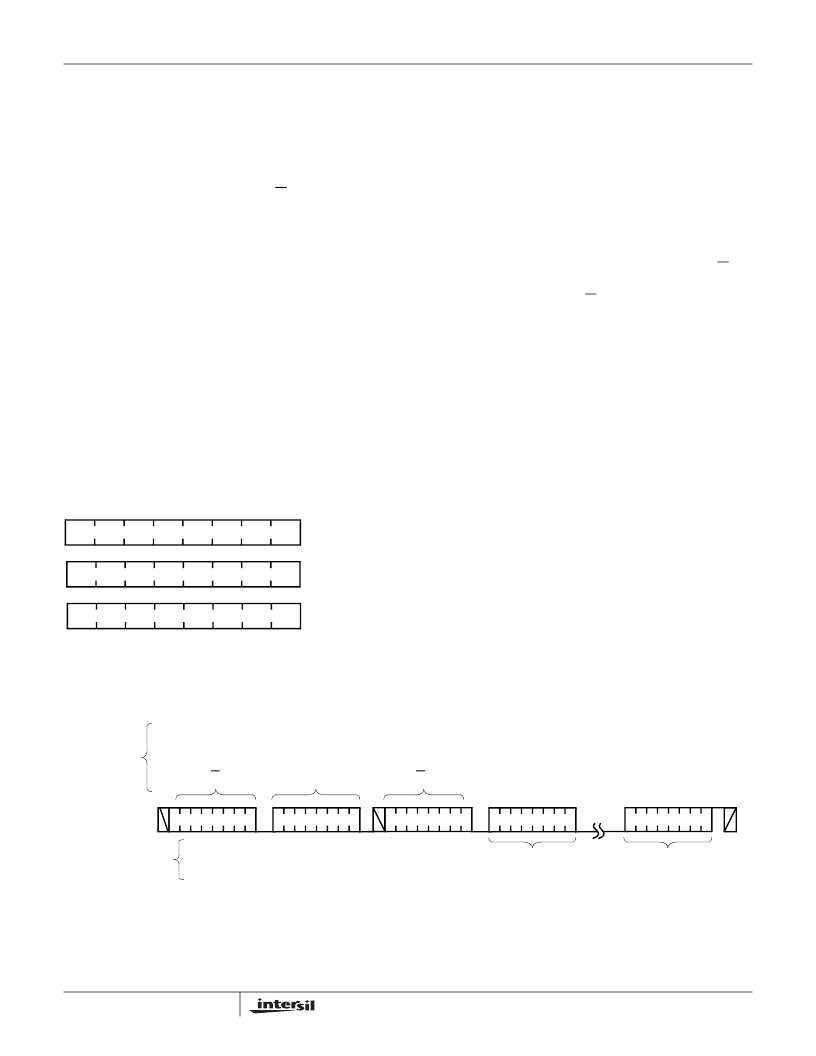
FIGURE 15. SLAVE ADDRESS, WORD ADDRESS, AND DATA
BYTES
SLAVE
ADDRESS BYTE
D7
D6
D5
D2
D4
D3
D1
D0
A0
A7
A2
A4
A3
A1
DATA BYTE
A6
A5
1
1
0
1
1
1
R/W
1
WORD ADDRESS
FIGURE 16. READ SEQUENCE
SIGNALS
FROM THE
MASTER
SIGNALS FROM
THE SLAVE
SIGNAL AT
SDA
S
T
A
R
T
IDENTIFICATION
BYTE WITH
R/W=0
ADDRESS
BYTE
A
C
K
A
C
K
0
S
T
O
P
A
C
K
1
IDENTIFICATION
BYTE WITH
R/W = 1
A
C
K
S
T
A
R
T
LAST READ
DATA BYTE
FIRST READ
DATA BYTE
A
C
K
1
0
1
1 1 1 1
1
0
1
1 1 1 1
ISL1220
相关PDF资料 |
PDF描述 |
|---|---|
| ISL1221 | Low Power RTC with Battery Backed SRAM and Event Detection(具有电池供电的SRAM和事件检测功能的低功率RTC) |
| ISL21009 | High Voltage Input Precision, Low Noise FGA Voltage References(高电压输入精度,低噪声FGA电压基准) |
| ISL21400 | Programmable Temperature Slope Voltage Reference(可编程温度斜率电压基准) |
| ISL22316 | Low Noise, Low Power I2C Bus, 128 Taps(低噪声,低功率,I2C总线, 128抽头电位器) |
| ISL22319 | Low Noise, Low Power, I2C Bus, 128 Taps, Wiper Only(低噪声,低功率,I2C总线, 128抽头电位器) |
相关代理商/技术参数 |
参数描述 |
|---|---|
| ISL1220IUZ | 功能描述:实时时钟 REAL TIME CLKRTC IN RoHS:否 制造商:Microchip Technology 功能:Clock, Calendar. Alarm RTC 总线接口:I2C 日期格式:DW:DM:M:Y 时间格式:HH:MM:SS RTC 存储容量:64 B 电源电压-最大:5.5 V 电源电压-最小:1.8 V 最大工作温度:+ 85 C 最小工作温度: 安装风格:Through Hole 封装 / 箱体:PDIP-8 封装:Tube |
| ISL1220IUZ-T | 功能描述:实时时钟 REAL TIME CLKRTC IN RoHS:否 制造商:Microchip Technology 功能:Clock, Calendar. Alarm RTC 总线接口:I2C 日期格式:DW:DM:M:Y 时间格式:HH:MM:SS RTC 存储容量:64 B 电源电压-最大:5.5 V 电源电压-最小:1.8 V 最大工作温度:+ 85 C 最小工作温度: 安装风格:Through Hole 封装 / 箱体:PDIP-8 封装:Tube |
| ISL1221 | 制造商:INTERSIL 制造商全称:Intersil Corporation 功能描述:Low Power RTC with Battery Backed |
| ISL1221IUZ | 功能描述:实时时钟 REAL TIME CLKRTC IN RoHS:否 制造商:Microchip Technology 功能:Clock, Calendar. Alarm RTC 总线接口:I2C 日期格式:DW:DM:M:Y 时间格式:HH:MM:SS RTC 存储容量:64 B 电源电压-最大:5.5 V 电源电压-最小:1.8 V 最大工作温度:+ 85 C 最小工作温度: 安装风格:Through Hole 封装 / 箱体:PDIP-8 封装:Tube |
| ISL1221IUZ-T | 功能描述:实时时钟 REAL TIME CLKRTC IN RoHS:否 制造商:Microchip Technology 功能:Clock, Calendar. Alarm RTC 总线接口:I2C 日期格式:DW:DM:M:Y 时间格式:HH:MM:SS RTC 存储容量:64 B 电源电压-最大:5.5 V 电源电压-最小:1.8 V 最大工作温度:+ 85 C 最小工作温度: 安装风格:Through Hole 封装 / 箱体:PDIP-8 封装:Tube |
发布紧急采购,3分钟左右您将得到回复。