- 您现在的位置:买卖IC网 > PDF目录383128 > ISL1220 (Intersil Corporation) Low Power RTC with 8 Bytes of Battery Backed SRAM and Separate FOUT(具有电池供电的8位SRAM和独立输出的低功率RTC) PDF资料下载
参数资料
| 型号: | ISL1220 |
| 厂商: | Intersil Corporation |
| 英文描述: | Low Power RTC with 8 Bytes of Battery Backed SRAM and Separate FOUT(具有电池供电的8位SRAM和独立输出的低功率RTC) |
| 中文描述: | 低功耗RTC与8电池供电SRAM和独立的FOUT(具有电池供电的8位的SRAM和独立输出的低功率实时时钟字节) |
| 文件页数: | 7/20页 |
| 文件大小: | 328K |
| 代理商: | ISL1220 |
7
FN6315.0
June 22, 2006
General Description
The ISL1220 device is a low power real time clock with
timing and crystal compensation, clock/calendar, power fail
indicator, periodic or polled alarm, intelligent battery backup
switching, battery-backed user SRAM and separate F
OUT
and IRQ outputs.
The oscillator uses an external, low-cost 32.768kHz crystal.
The real time clock tracks time with separate registers for
hours, minutes, and seconds. The device has calendar
registers for date, month, year and day of the week. The
calendar is accurate through 2099, with automatic leap year
correction.
The ISL1220's powerful alarm can be set to any
clock/calendar value for a match. For example, every
minute, every Tuesday or at 5:23 AM on March 21. The
alarm status is available by checking the Status Register, or
the device can be configured to provide a hardware interrupt
via the IRQ pin. There is a repeat mode for the alarm
allowing a periodic interrupt every minute, every hour, every
day, etc.
The device also offers a backup power input pin. This V
BAT
pin allows the device to be backed up by battery or Super
Cap with automatic switchover from V
DD
to V
BAT
. The entire
ISL1220 device is fully operational from 2.0V to 5.5V and the
clock/calendar portion of the device remains fully operational
down to 1.8V (Standby Mode).
Pin Description
X1, X2
The X1 and X2 pins are the input and output, respectively, of
an inverting amplifier. An external 32.768kHz quartz crystal
is used with the ISL1220 to supply a timebase for the real
time clock. Internal compensation circuitry provides high
accuracy over the operating temperature range from
-40°C to +85°C. This oscillator compensation network can
be used to calibrate the crystal timing accuracy over
temperature either during manufacturing or with an external
temperature sensor and microcontroller for active
compensation. The device can also be driven directly from a
32.768kHz source at pin X1.
V
BAT
This input provides a backup supply voltage to the device.
V
BAT
supplies power to the device in the event that the V
DD
supply fails. This pin can be connected to a battery, a Super
Cap or tied to ground if not used.
IRQ (Interrupt Output)
The IRQ output is an open drain active low configuration.
Interrupt Mode.
The pin provides an interrupt signal
output. This signal notifies a host processor that an alarm
has occurred and requests action. It is an open drain
active low output.
Serial Clock (SCL)
The SCL input is used to clock all serial data into and out of
the device. The input buffer on this pin is always active (not
gated). It is disabled when the backup power supply on the
V
BAT
pin is activated to minimize power consumption.
Serial Data (SDA)
SDA is a bidirectional pin used to transfer data into and out
of the device. It has an open drain output and may be ORed
with other open drain or open collector outputs. The input
buffer is always active (not gated) in normal mode.
An open drain output requires the use of a pull-up resistor.
The output circuitry controls the fall time of the output signal
with the use of a slope controlled pull-down. The circuit is
designed for 400kHz I
2
C interface speeds. It is disabled
when the backup power supply on the V
BAT
pin is activated.
F
OUT
(Frequency Output)
Frequency Output Mode.
The pin outputs a clock signal
which is related to the crystal frequency. The frequency
output is user selectable and enabled via the I
2
C bus. It is
an open drain active low output.
V
DD
, GND
Chip power supply and ground pins. The device will operate
with a power supply from 2.0V to 5.5VDC. A 0.1μF capacitor
is recommended on the V
DD
pin to ground.
Functional Description
Power Control Operation
The power control circuit accepts a V
DD
and a V
BAT
input.
Many types of batteries can be used with Intersil RTC
products. For example, 3.0V or 3.6V Lithium batteries are
appropriate, and battery sizes are available that can power
the ISL1220 for up to 10 years. Another option is to use a
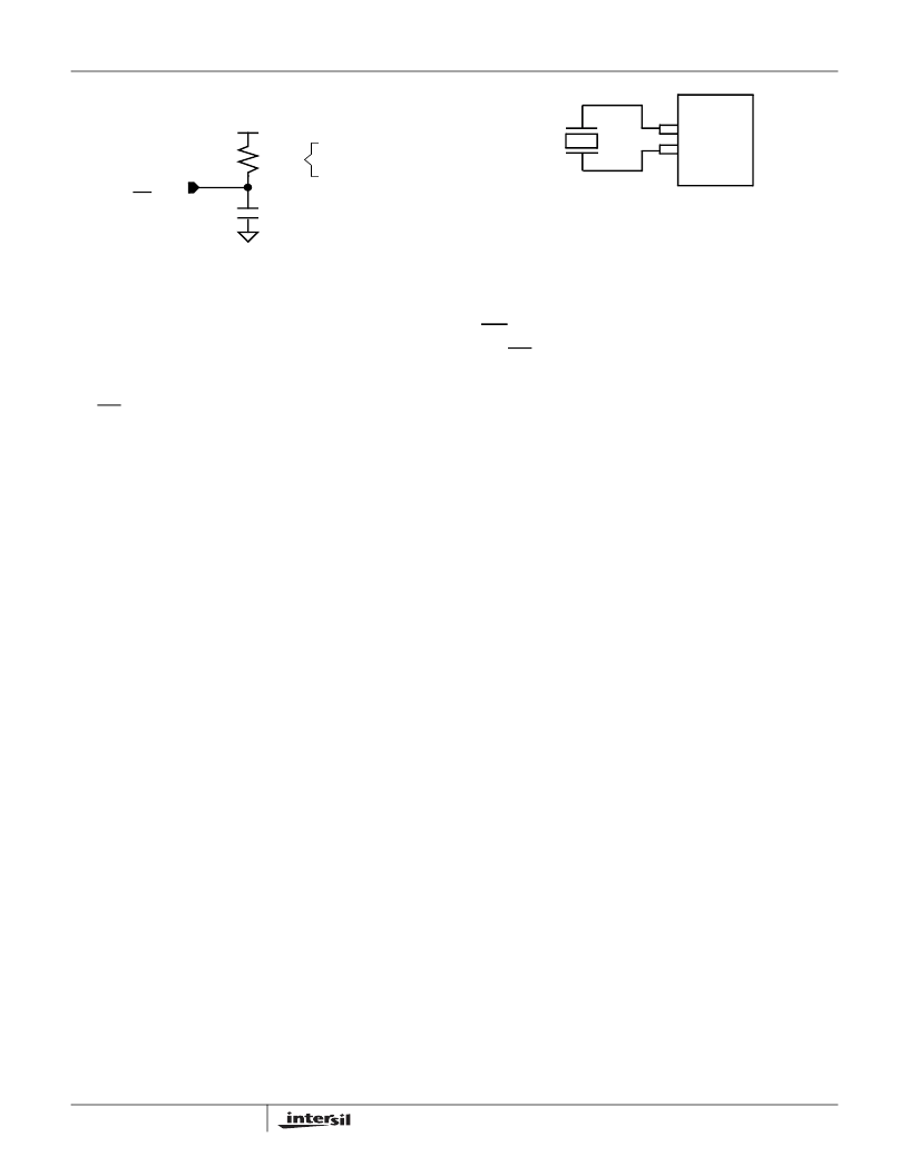
FIGURE 7. STANDARD OUTPUT LOAD FOR TESTING THE
DEVICE WITH V
DD
= 5.0V
SDA
AND
IRQ, F
OUT
1533
100pF
5.0V
FOR V
OL
= 0.4V
AND I
OL
= 3mA
EQUIVALENT AC OUTPUT LOAD CIRCUIT FOR V
DD
= 5V
FIGURE 8. RECOMMENDED CRYSTAL CONNECTION
X1
X2
ISL1220
相关PDF资料 |
PDF描述 |
|---|---|
| ISL1221 | Low Power RTC with Battery Backed SRAM and Event Detection(具有电池供电的SRAM和事件检测功能的低功率RTC) |
| ISL21009 | High Voltage Input Precision, Low Noise FGA Voltage References(高电压输入精度,低噪声FGA电压基准) |
| ISL21400 | Programmable Temperature Slope Voltage Reference(可编程温度斜率电压基准) |
| ISL22316 | Low Noise, Low Power I2C Bus, 128 Taps(低噪声,低功率,I2C总线, 128抽头电位器) |
| ISL22319 | Low Noise, Low Power, I2C Bus, 128 Taps, Wiper Only(低噪声,低功率,I2C总线, 128抽头电位器) |
相关代理商/技术参数 |
参数描述 |
|---|---|
| ISL1220IUZ | 功能描述:实时时钟 REAL TIME CLKRTC IN RoHS:否 制造商:Microchip Technology 功能:Clock, Calendar. Alarm RTC 总线接口:I2C 日期格式:DW:DM:M:Y 时间格式:HH:MM:SS RTC 存储容量:64 B 电源电压-最大:5.5 V 电源电压-最小:1.8 V 最大工作温度:+ 85 C 最小工作温度: 安装风格:Through Hole 封装 / 箱体:PDIP-8 封装:Tube |
| ISL1220IUZ-T | 功能描述:实时时钟 REAL TIME CLKRTC IN RoHS:否 制造商:Microchip Technology 功能:Clock, Calendar. Alarm RTC 总线接口:I2C 日期格式:DW:DM:M:Y 时间格式:HH:MM:SS RTC 存储容量:64 B 电源电压-最大:5.5 V 电源电压-最小:1.8 V 最大工作温度:+ 85 C 最小工作温度: 安装风格:Through Hole 封装 / 箱体:PDIP-8 封装:Tube |
| ISL1221 | 制造商:INTERSIL 制造商全称:Intersil Corporation 功能描述:Low Power RTC with Battery Backed |
| ISL1221IUZ | 功能描述:实时时钟 REAL TIME CLKRTC IN RoHS:否 制造商:Microchip Technology 功能:Clock, Calendar. Alarm RTC 总线接口:I2C 日期格式:DW:DM:M:Y 时间格式:HH:MM:SS RTC 存储容量:64 B 电源电压-最大:5.5 V 电源电压-最小:1.8 V 最大工作温度:+ 85 C 最小工作温度: 安装风格:Through Hole 封装 / 箱体:PDIP-8 封装:Tube |
| ISL1221IUZ-T | 功能描述:实时时钟 REAL TIME CLKRTC IN RoHS:否 制造商:Microchip Technology 功能:Clock, Calendar. Alarm RTC 总线接口:I2C 日期格式:DW:DM:M:Y 时间格式:HH:MM:SS RTC 存储容量:64 B 电源电压-最大:5.5 V 电源电压-最小:1.8 V 最大工作温度:+ 85 C 最小工作温度: 安装风格:Through Hole 封装 / 箱体:PDIP-8 封装:Tube |
发布紧急采购,3分钟左右您将得到回复。