- 您现在的位置:买卖IC网 > PDF目录383128 > ISL21400 (Intersil Corporation) Programmable Temperature Slope Voltage Reference(可编程温度斜率电压基准) PDF资料下载
参数资料
| 型号: | ISL21400 |
| 厂商: | Intersil Corporation |
| 英文描述: | Programmable Temperature Slope Voltage Reference(可编程温度斜率电压基准) |
| 中文描述: | 可编程温度斜坡电压基准(可编程温度斜率电压基准) |
| 文件页数: | 11/17页 |
| 文件大小: | 439K |
| 代理商: | ISL21400 |
11
FN8091.1
April 24, 2007
Register Descriptions
Register 0: Bandgap Reference Gain (Nonvolatile)
Register 0 sets the output voltage of the bandgap reference
(V
REF
). Referring to Equation 1, the number “n” is the setting
from Register 0 as follows:
This term of Equation 1 can vary from 0V to 1.20V.
Register 1: Temperature Slope Gain (Nonvolatile)
Register 1 sets the Temperature Slope (TS) of the
temperature sensor. Referring to Equation 1, the number “m”
is the setting from Register 1 as follows:
V
TS
is the temperature dependent term and varies from
+136mV at -40°C to -126mV at +85°C. The other term varies
from -1 to +1 and scales the temperature term before adding
to the V
REF
portion.
Register 2: Device Gain and Storage (nonvolatile)
Register 2 contains 2 bits (2 LSB’s) which control the output
gain of the device. Table 3 shows the state of these two bits
and the resulting output gain. Note that two states produce
the same gain (Gain 1:0 set to 01b and 10b) of x2.
The other 6-bits in the register can be used for general
purpose memory (nonvolatile) or left alone.
Registers 3 and 4: general purpose data
(nonvolatile)
These two registers are one byte each and can be used for
general purpose nonvolatile memory.
I
2
C Serial Interface
The ISL21400 supports a bidirectional bus oriented protocol.
The protocol defines any device that sends data onto the
bus as a transmitter and the receiving device as the receiver.
The device controlling the transfer is the master and the
device being controlled is the slave. The master always
initiates data transfers and provides the clock for both
transmit and receive operations. Therefore, the ISL21400
operates as a slave device in all applications.
All communication over the I
2
C interface is conducted by
sending the MSB of each byte of data first.
Protocol Conventions
Data states on the SDA line can change only during SCL
LOW periods. SDA state changes during SCL HIGH are
reserved for indicating START and STOP conditions (See
Figure 10). On power-up of the ISL21400 the SDA pin is in
the input mode.
All I
2
C interface operations must begin with a START
condition, which is a HIGH to LOW transition of SDA while
SCL is HIGH. The ISL21400 continuously monitors the SDA
and SCL lines for the START condition and does not
respond to any command until this condition is met (See
Figure 10). A START condition is ignored during the power-
up sequence and during non-volatile write cycles for the
device.
All I
2
C interface operations must be terminated by a STOP
condition, which is a LOW to HIGH transition of SDA while
SCL is HIGH (See Figure 10) A STOP condition at the end of
a read operation, or at the end of a write operation places
the device in its standby mode. A STOP condition at the end
of a write operation to a non-volatile byte initiates an internal
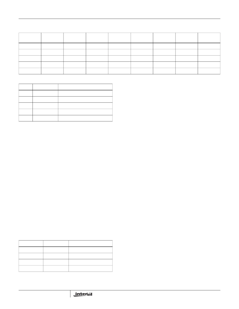
TABLE 1. ISL21400 REGISTER BIT MAP
Addr
D7
(MSB)
D6
D5
D4
D3
D2
D1
D0
(LSB)
0
V
REF
7
V
REF
6
V
REF
5
V
REF
4
V
REF
3
V
REF
2
V
REF
1
V
REF
0
1
TS7
TS6
TS5
TS4
TS3
TS2
TS1
TS0
2
D7
D6
D5
D4
D3
D2
GAIN1
GAIN0
3
D7
D6
D5
D4
D3
D2
D1
D0
4
D7
D6
D5
D4
D3
D2
D1
D0
TABLE 2. REGISTER DESCRIPTIONS
REG
NONVOLATILE
DESCRIPTION
0
Y
Reference setting
1
Y
Temperature Sensor setting
2
Y
Gain and storage
3
Y
Storage
4
Y
Storage
TABLE 3. REGISTER 2 OUTPUT GAIN (NONVOLATILE):
OUTPUT GAIN
GAIN1
GAIN0
OUTPUT GAIN, A
V
0
0
x 1
0
1
x 2
1
0
x 2
1
1
x 4
V
REF
---------
, for n = 0 to 255
V
TS
------------------–
ISL21400
相关PDF资料 |
PDF描述 |
|---|---|
| ISL22316 | Low Noise, Low Power I2C Bus, 128 Taps(低噪声,低功率,I2C总线, 128抽头电位器) |
| ISL22319 | Low Noise, Low Power, I2C Bus, 128 Taps, Wiper Only(低噪声,低功率,I2C总线, 128抽头电位器) |
| ISL22326 | Low Noise, Low Power, I2C Bus, 128 Taps(低噪声,低功率,I2C总线, 128抽头电位器) |
| ISL22329 | Low Noise, Low Power, I2C Bus, 128 Taps, Wiper Only(低噪声,低功率,I2C总线, 128抽头电位器) |
| ISL22346 | Low Noise, Low Power I2C Bus, 128 Taps(低噪声,低功率,I2C总线, 128抽头电位器) |
相关代理商/技术参数 |
参数描述 |
|---|---|
| ISL21400IU8Z | 功能描述:基准电压& 基准电流 ISL21400IU8ZISE VAGEFERENCE W/PTAT RoHS:否 制造商:STMicroelectronics 产品:Voltage References 拓扑结构:Shunt References 参考类型:Programmable 输出电压:1.24 V to 18 V 初始准确度:0.25 % 平均温度系数(典型值):100 PPM / C 串联 VREF - 输入电压(最大值): 串联 VREF - 输入电压(最小值): 分流电流(最大值):60 mA 最大工作温度:+ 125 C 封装 / 箱体:SOT-23-3L 封装:Reel |
| ISL21400IU8Z-TK | 功能描述:基准电压& 基准电流 ISL21400IU8ZISE VAGEFERENCE W/PTAT RoHS:否 制造商:STMicroelectronics 产品:Voltage References 拓扑结构:Shunt References 参考类型:Programmable 输出电压:1.24 V to 18 V 初始准确度:0.25 % 平均温度系数(典型值):100 PPM / C 串联 VREF - 输入电压(最大值): 串联 VREF - 输入电压(最小值): 分流电流(最大值):60 mA 最大工作温度:+ 125 C 封装 / 箱体:SOT-23-3L 封装:Reel |
| ISL21400USB-EVALZ | 功能描述:电源管理IC开发工具 ISL21400USB-EVALZ BRD ROHS COMPLAINT RoHS:否 制造商:Maxim Integrated 产品:Evaluation Kits 类型:Battery Management 工具用于评估:MAX17710GB 输入电压: 输出电压:1.8 V |
| ISL21440 | 制造商:INTERSIL 制造商全称:Intersil Corporation 功能描述:Micropower Voltage Reference with Comparator |
| ISL21440_11 | 制造商:INTERSIL 制造商全称:Intersil Corporation 功能描述:Micropower Voltage Reference with Comparator |
发布紧急采购,3分钟左右您将得到回复。