- 您现在的位置:买卖IC网 > PDF目录383128 > ISL21400 (Intersil Corporation) Programmable Temperature Slope Voltage Reference(可编程温度斜率电压基准) PDF资料下载
参数资料
| 型号: | ISL21400 |
| 厂商: | Intersil Corporation |
| 英文描述: | Programmable Temperature Slope Voltage Reference(可编程温度斜率电压基准) |
| 中文描述: | 可编程温度斜坡电压基准(可编程温度斜率电压基准) |
| 文件页数: | 12/17页 |
| 文件大小: | 439K |
| 代理商: | ISL21400 |
12
FN8091.1
April 24, 2007
non-volatile write cycle. The device enters its standby state
when the internal, non-volatile write cycle is completed.
An ACK, Acknowledge, is a software convention used to
indicate a successful data transfer. The transmitting device,
either master or slave, releases the SDA bus after
transmitting eight bits. During the ninth clock cycle, the
receiver pulls the SDA line LOW to acknowledge the
reception of the eight bits of data (See Figure 11).
The ISL21400 responds with an ACK after recognition of a
START condition followed by a valid Identification Byte, and
once again after successful receipt of an Address Byte. The
ISL21400 also responds with an ACK after receiving a Data
Byte of a write operation. The master must respond with an
ACK after receiving a Data Byte of a read operation.
A valid Identification Byte contains 0101 A2 A1 A0 as the
seven MSBs. The A2 A1 A0 bits must correspond to the
logic levels at those pins of the ISL21400 device. The LSB in
the Read/Write bit. Its value is “1” for a Read operation, and
“0” for a Write operation (See Table 4).
Write Operation
A Write operation requires a START condition, followed by a
valid Identification Byte, a valid Address Byte, a Data Byte,
and a STOP condition. After each of the three bytes, the
ISL21400 responds with an ACK. The master will then send
a STOP and at this time the device begins its internal
non-volatile write cycle. During this time, the device ignores
transitions at the SDA and SCL pins, and the SDA output is
at a high impedance state. When the internal non-volatile
write cycle is completed, the ISL21400 enters its standby
state (see Figure 12).
STOP conditions that terminate write operations must be
sent by the master after sending at least 1 full data byte and
its associated ACK signal. If a STOP byte is issued in the
middle of a data byte, or before 1 full data byte + ACK is
sent, then the ISL21400 resets itself without performing the
write. The contents of the array are not affected.
Data Protection
A valid Identification Byte, Address Byte, and total number of
SCL pulses act as a protection for the registers. A STOP
condition also acts as a protection for non-volatile memory.
During a Write sequence, the Data Byte is loaded into an
internal shift register as it is received. The presence of the
STOP condition after the rest of the bits are received then
triggers the non-volatile write.
Read Operation
A Current Address Read operation is shown in Figure 13. It
consists of a minimum 2 bytes: a START followed by the ID
byte from the master with the R/W bit set to 1, then an ACK
followed by the data byte or bytes sent by the slave. The
master terminates the Read operation by not responding
with an ACK and then issuing a STOP condition. This
operation is useful if the master knows the current address
and desires to read one or more data bytes.
A Random Address Read operation consists of a three byte
“dummy write” instruction followed by a Current Address
Read operation (See Figure 14). The master initiates the
operation issuing the following sequence: a START, the
identification byte with the R/W bit set to "0", an Address
Byte, a second START, and a second Identification byte with
the R/W bit set to "1". After each of the three bytes, the
ISL21400 responds with an ACK. The ISL21400 then
transmits Data Bytes as long as the master responds with an
ACK during the SCL cycle following the eighth bit of each
byte. The master terminates the Read operation (issuing a
STOP condition) following the last bit of the last Data Byte
(See Figure 13).
The Data Bytes are from the registers indicated by an
internal pointer. This pointer initial’s value is determined by
the Address Byte in the Read operation instruction, and
increments by one during transmission of each Data Byte.
Address 04h is the last valid data byte, higher addresses are
not available. Data from addresses higher than memory
location 04h will be invalid.
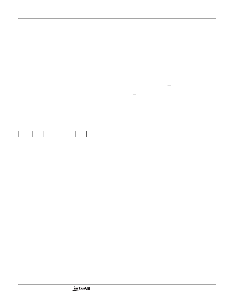
TABLE 4. IDENTIFICATION BYTE FORMAT
0
1
0
1
A2
A1
A0
R/W
(MSB)
(LSB)
ISL21400
相关PDF资料 |
PDF描述 |
|---|---|
| ISL22316 | Low Noise, Low Power I2C Bus, 128 Taps(低噪声,低功率,I2C总线, 128抽头电位器) |
| ISL22319 | Low Noise, Low Power, I2C Bus, 128 Taps, Wiper Only(低噪声,低功率,I2C总线, 128抽头电位器) |
| ISL22326 | Low Noise, Low Power, I2C Bus, 128 Taps(低噪声,低功率,I2C总线, 128抽头电位器) |
| ISL22329 | Low Noise, Low Power, I2C Bus, 128 Taps, Wiper Only(低噪声,低功率,I2C总线, 128抽头电位器) |
| ISL22346 | Low Noise, Low Power I2C Bus, 128 Taps(低噪声,低功率,I2C总线, 128抽头电位器) |
相关代理商/技术参数 |
参数描述 |
|---|---|
| ISL21400IU8Z | 功能描述:基准电压& 基准电流 ISL21400IU8ZISE VAGEFERENCE W/PTAT RoHS:否 制造商:STMicroelectronics 产品:Voltage References 拓扑结构:Shunt References 参考类型:Programmable 输出电压:1.24 V to 18 V 初始准确度:0.25 % 平均温度系数(典型值):100 PPM / C 串联 VREF - 输入电压(最大值): 串联 VREF - 输入电压(最小值): 分流电流(最大值):60 mA 最大工作温度:+ 125 C 封装 / 箱体:SOT-23-3L 封装:Reel |
| ISL21400IU8Z-TK | 功能描述:基准电压& 基准电流 ISL21400IU8ZISE VAGEFERENCE W/PTAT RoHS:否 制造商:STMicroelectronics 产品:Voltage References 拓扑结构:Shunt References 参考类型:Programmable 输出电压:1.24 V to 18 V 初始准确度:0.25 % 平均温度系数(典型值):100 PPM / C 串联 VREF - 输入电压(最大值): 串联 VREF - 输入电压(最小值): 分流电流(最大值):60 mA 最大工作温度:+ 125 C 封装 / 箱体:SOT-23-3L 封装:Reel |
| ISL21400USB-EVALZ | 功能描述:电源管理IC开发工具 ISL21400USB-EVALZ BRD ROHS COMPLAINT RoHS:否 制造商:Maxim Integrated 产品:Evaluation Kits 类型:Battery Management 工具用于评估:MAX17710GB 输入电压: 输出电压:1.8 V |
| ISL21440 | 制造商:INTERSIL 制造商全称:Intersil Corporation 功能描述:Micropower Voltage Reference with Comparator |
| ISL21440_11 | 制造商:INTERSIL 制造商全称:Intersil Corporation 功能描述:Micropower Voltage Reference with Comparator |
发布紧急采购,3分钟左右您将得到回复。