- 您现在的位置:买卖IC网 > PDF目录383128 > ISL21400 (Intersil Corporation) Programmable Temperature Slope Voltage Reference(可编程温度斜率电压基准) PDF资料下载
参数资料
| 型号: | ISL21400 |
| 厂商: | Intersil Corporation |
| 英文描述: | Programmable Temperature Slope Voltage Reference(可编程温度斜率电压基准) |
| 中文描述: | 可编程温度斜坡电压基准(可编程温度斜率电压基准) |
| 文件页数: | 14/17页 |
| 文件大小: | 439K |
| 代理商: | ISL21400 |
14
FN8091.1
April 24, 2007
Applications Information
Power-Up Considerations
The ISL21400 has on-chip EEPROM memory storage for
the DAC and gain settings of the device. These settings
must be recalled correctly on power-up for proper operation.
Normally there are no issues with recall, although it is always
best to provide a smooth, glitch-free power-up waveform on
V
CC
. Adding a small 0.1
μ
F capacitor at the device V
CC
will
help with power-up as well as V
OUT
load changes.
Noise Performance
The output noise voltage in a 0.1Hz to 10Hz bandwidth is
typically 90μV
P-P
. The noise measurement is made with a
bandpass filter made of a 1 pole high-pass filter with a corner
frequency at 0.1Hz and a 2-pole low-pass filter with a corner
frequency at 12.6Hz to create a filter with a 9.9Hz
bandwidth. Load capacitance up to 5000pF can be added
but will result in only marginal improvements in output noise
and transient response. The output stage of the ISL21400 is
not designed to drive heavily capacitive loads. For high
impedance loads, an R-C network can be added to filter high
frequency noise and preserve DC control.
Output Voltage Programming Considerations
Setting and controlling the output voltage of the ISL21400
can be done easily by breaking down the components into
temperature variant and invariant, and setting them
separately. Let’s use Equation 1 to derive separate
Reference Output and Output Temp Slope equations:
The first term controls the output DC value, and the second
term controls the Temp slope, where
DC OUTPUT CONTROL DISCUSSION
The reference term yields Equation 2 for Reference Output:
Note that the DC term is dependent on the 1.20V reference
voltage, which is constant, the overall gain, A
V
, and the
Reference gain, A
REF
. Since the product A
V
* A
REF
ranges
from 0 to 4, the total reference DC output can range from
0.0V to 4.8V. In order to get the 4.8V output, V
CC
must be
greater than 4.8V by the output dropout plus any overhead
for output loading (the specification for V
OUT
= 5.0V is listed
with V
CC
= 5.5V). The Resolution of V
OUT
(DC) control
changes with A
V
, so that with a 4.80V full scale output
(A
V
= 4), the resolution is 4.80/255 or 18.8mV/bit. With
A
V
= 1, the resolution is 4.7mV/bit.
TEMP SENSE CONTROL DISCUSSION
Equation 2 yields this expression, Equation 3, for Temp
Slope:
Since V
TS
= K(T - T
0
), the slope term is dependent on the
base temp slope of the device, K (-2.1mV/°C), and the gain
terms A
V
and A
TS
. This gives a formula (Equation 4) for the
portion of V
OUT
at a specific temperature:
The product A
V
*A
TS
ranges from -4 to 4, so the Temperature
Slope can range from -8.4 to +8.4mV/°C, which is
independent of the output DC voltage. The resolution of
Slope control is determined by this range (±8.4mV/°C) and
the gain terms, and will vary from 65.8
μ
V/°C/bit (A
V
= 4)
down to 16.2
μ
V/°C/bit (A
V
= 1).
At T = T
0
= +25°C, V
OUT
(TS) = 0, no changes in A
TS
will
cause a change in V
OUT
, and V
OUT
will only vary with the
V
OUT
(DC) control. As temperature increases or decreases,
from T = +25°C, V
OUT
will then change according to the
programmed Temp Slope.
SIGNALS
FROM THE
MASTER
SIGNALS FROM
THE SLAVE
SIGNAL AT SDA
S
T
A
R
T
IDENTIFICATION
BYTE WITH R/W = 0
ADDRESS
BYTE
A
C
K
A
C
K
0
0
0
1
1
S
T
O
P
A
C
K
0
1
0
1
1
IDENTIFICATION
BYTE WITH R/W = 1
A
C
K
S
T
A
R
T
LAST READ
DATA BYTE
FIRST READ
DATA BYTE
A
C
K
A
A
A
0
0 0 0
0
A A A
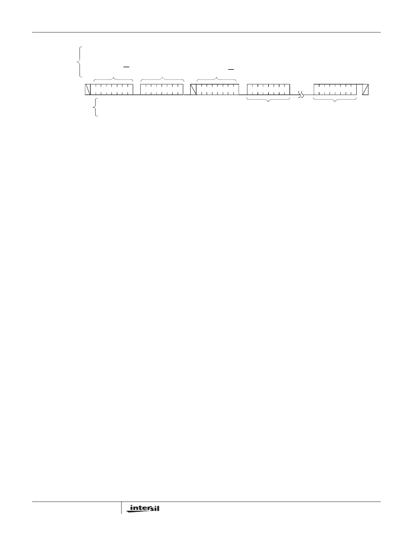
FIGURE 18. RANDOM ADDRESS READ SEQUENCE
V
OUT
A
V
V
REF
---------
{
A
V
V
TS
-------------------–
+
=
A
V
V
REF
A
REF
}
=
A
V
V
TS
A
TS
{
}
""
+
Reference Term
Temp Slope Term
+
A
REF
---------
=
(ranges from 0 to 1)
A
TS
-------------------–
(ranges from -1 to +1)
=
V
OUT
(DC)
A
=
V
V
REF
A
REF
(EQ. 2)
V
OUT
TS
(
)
A
V
V
TS
A
TS
=
(EQ. 3)
V
OUT
TS
(
)
A
V
K
A
TS
T
T
0
–
(
)
=
(EQ. 4)
ISL21400
相关PDF资料 |
PDF描述 |
|---|---|
| ISL22316 | Low Noise, Low Power I2C Bus, 128 Taps(低噪声,低功率,I2C总线, 128抽头电位器) |
| ISL22319 | Low Noise, Low Power, I2C Bus, 128 Taps, Wiper Only(低噪声,低功率,I2C总线, 128抽头电位器) |
| ISL22326 | Low Noise, Low Power, I2C Bus, 128 Taps(低噪声,低功率,I2C总线, 128抽头电位器) |
| ISL22329 | Low Noise, Low Power, I2C Bus, 128 Taps, Wiper Only(低噪声,低功率,I2C总线, 128抽头电位器) |
| ISL22346 | Low Noise, Low Power I2C Bus, 128 Taps(低噪声,低功率,I2C总线, 128抽头电位器) |
相关代理商/技术参数 |
参数描述 |
|---|---|
| ISL21400IU8Z | 功能描述:基准电压& 基准电流 ISL21400IU8ZISE VAGEFERENCE W/PTAT RoHS:否 制造商:STMicroelectronics 产品:Voltage References 拓扑结构:Shunt References 参考类型:Programmable 输出电压:1.24 V to 18 V 初始准确度:0.25 % 平均温度系数(典型值):100 PPM / C 串联 VREF - 输入电压(最大值): 串联 VREF - 输入电压(最小值): 分流电流(最大值):60 mA 最大工作温度:+ 125 C 封装 / 箱体:SOT-23-3L 封装:Reel |
| ISL21400IU8Z-TK | 功能描述:基准电压& 基准电流 ISL21400IU8ZISE VAGEFERENCE W/PTAT RoHS:否 制造商:STMicroelectronics 产品:Voltage References 拓扑结构:Shunt References 参考类型:Programmable 输出电压:1.24 V to 18 V 初始准确度:0.25 % 平均温度系数(典型值):100 PPM / C 串联 VREF - 输入电压(最大值): 串联 VREF - 输入电压(最小值): 分流电流(最大值):60 mA 最大工作温度:+ 125 C 封装 / 箱体:SOT-23-3L 封装:Reel |
| ISL21400USB-EVALZ | 功能描述:电源管理IC开发工具 ISL21400USB-EVALZ BRD ROHS COMPLAINT RoHS:否 制造商:Maxim Integrated 产品:Evaluation Kits 类型:Battery Management 工具用于评估:MAX17710GB 输入电压: 输出电压:1.8 V |
| ISL21440 | 制造商:INTERSIL 制造商全称:Intersil Corporation 功能描述:Micropower Voltage Reference with Comparator |
| ISL21440_11 | 制造商:INTERSIL 制造商全称:Intersil Corporation 功能描述:Micropower Voltage Reference with Comparator |
发布紧急采购,3分钟左右您将得到回复。