- 您现在的位置:买卖IC网 > PDF目录383135 > ISL5586CIM (INTERSIL CORP) Low Power Ringing SLIC for Home Gateways PDF资料下载
参数资料
| 型号: | ISL5586CIM |
| 厂商: | INTERSIL CORP |
| 元件分类: | 模拟传输电路 |
| 英文描述: | Low Power Ringing SLIC for Home Gateways |
| 中文描述: | TELECOM-SLIC, PQCC28 |
| 封装: | PLASTIC, MS-018AB, LCC-28 |
| 文件页数: | 7/20页 |
| 文件大小: | 497K |
| 代理商: | ISL5586CIM |
4-7
4-WIRE TO 2-WIRE GAIN
The 4-wire to 2-wire gain (G
42
) is defined as the receive
gain. It is a function of the terminating impedance,
synthesized impedance and protection resistors. The gain is
defined from the Receive input terminals (V
RXP
, V
RXM
) to
the terminating impedance (Z
L
) on the 2-wire side, and is
illustrated in Figure 12.
When the device source impedance and the protection
resistors equal the terminating impedance, the receive gain
equals 2.92dB and is inverted with respect to the input.
2-WIRE TO 4-WIRE GAIN
The 2-wire to 4-wire gain (G
24
) is the gain from tip and ring to
the transmit differential output. The transmit gain is given by
Equation 11. Note that V
TR
is defined on the line side of the
protection resistors (reference Figure 13). With Z
L
set to 600
ohms, the protection resistors set to 50
/terminal and
Z
0
= Z
L
-2RP the Transmit gain equals -0.833 (-1.59dB) and
is inverted with respect to the 2-wire input (V
TR
).
TRANSHYBRID GAIN
The transhybrid gain is defined as the 4-wire to 4-wire gain
(G
44
) and is given by Equation 12 (Reference Figure 14)).
Transient Current Limit
The drive current capability of the output amplifiers is
determined by an externally programmable output current
limit circuit which is separate from the DC loop current limit
function. The transient current limit is programmed with a
resistor to ground at the TL pin. The current limit circuit
works in both the source and sink direction, with an internally
fixed offset to prevent the current limit functions from turning
on simultaneously. The current limit function is provided by
sensing line current and reducing the voltage drive to the
load when the externally set threshold is exceeded, hence
forcing a constant source or sink current.
SOURCE CURRENT PROGRAMMING
The source current is externally programmed as shown in
Equation 13.
For example, a source current limit setting of 50mA is
programmed with a 35.6k
resistor connected from pin 16 of
the device to ground. This setting determines the maximum
amount of current which flows from Tip to Ring during an off
hook event until the DC loop current limit responds. In addition
this setting also determines the amount of current which will
flow from Tip or Ring when external battery faults occur.
SINK CURRENT PROGRAMMING
The sink current limit is internally offset 20% higher than the
externally programmed source current limit setting.
If the source current limit is set to 50mA, the sink current limit
will be 60mA. This setting will determine the amount of current
which flows into Tip or Ring when external ground faults occur.
FUNCTIONAL DESCRIPTION
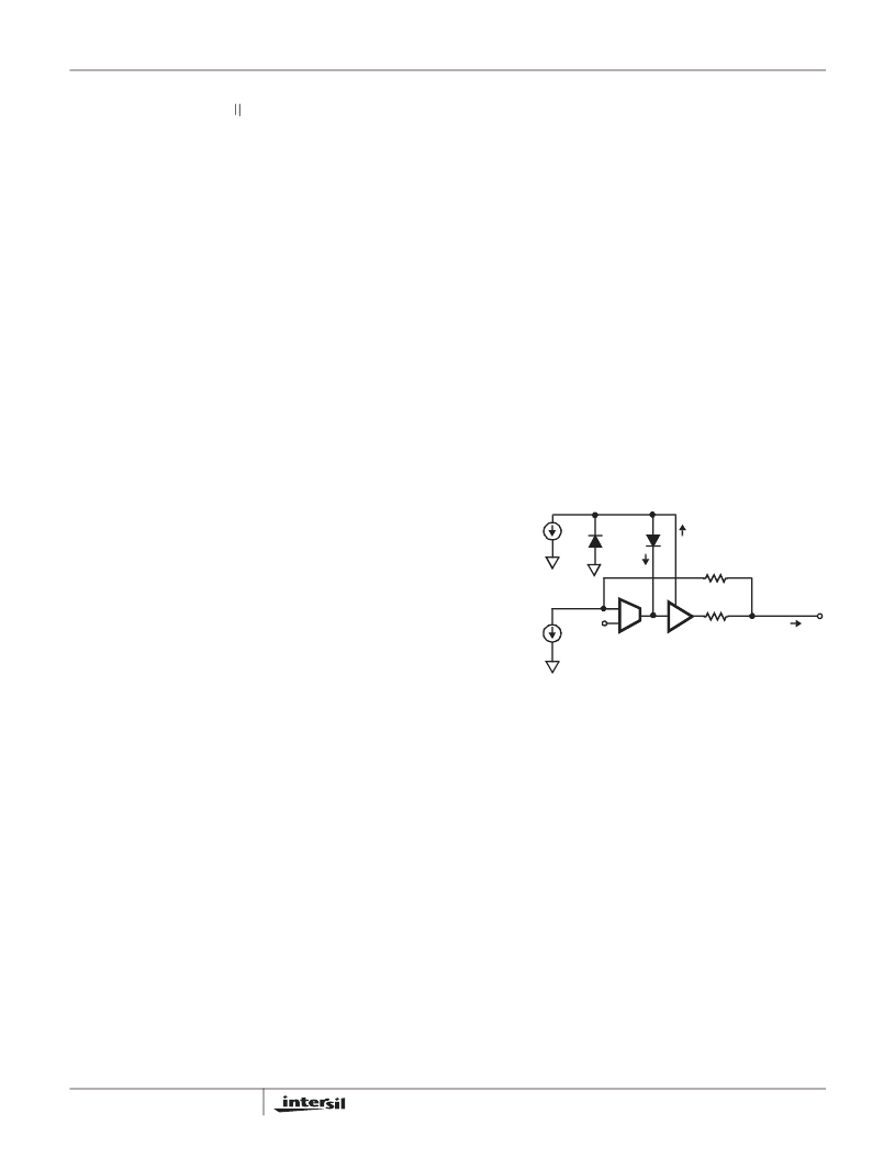
Each amplifier is designed to limit source current and sink
current. The diagram below shows the functionality of the
circuit for the case of limiting the source current. A similar
diagram applies to the sink current limit with current polarity
changed accordingly.
During normal operation, the error current (I
ERR
) is zero and
the output voltage is determined by the signal current (I
SIG
)
multiplied by the 200K feedback resistor. With the current
polarity as shown for I
SIG
, the output voltage moves positive
with respect to half battery. Assuming the amplifier output is
driving a load at a more negative potential, the amplifier
output will source current.
During excessive output source current flow, the scaled
output current (I
O
/K) exceeds the reference current (I
REF
)
forcing an error current (I
ERR
). With the polarity as shown
the error current subtracts from the signal current, which
reduces the amplifier output voltage. By reducing the output
voltage the source current to the load is decreased and the
output current is limited.
DETERMINING THE PROPER SETTING
Since this feature programs the maximum output current of
the device, the setting must be high enough to allow for
detection of ring trip or programmed off hook loop current,
whichever is greater.
Z
O
R1
RP1
–
RP2
–
(
)
R2 C2
+
=
(EQ. 9)
G
42
2.8
Z
O
P
L
-----------------------------------------
–
=
(EQ. 10)
G
24
2
Z
O
P
L
-----------------------------------------
–
=
(EQ. 11)
G
44
2.8
Z
P
O
L
+
----------+
–
=
(EQ. 12)
R
TL
SRC
-------------
=
(EQ. 13)
I
SNK
1.20
I
SRC
×
=
(EQ. 14)
FIGURE 2. CURRENT LIMIT FUNCTIONAL DIAGRAM
TIP or RING
+
-
I
REF
= 1.21/TL
I
O
I
O
/K
I
ERR
I
SIG
20
200K
VB/2
ISL5586
相关PDF资料 |
PDF描述 |
|---|---|
| ISL5586DIM | Low Power Ringing SLIC for Home Gateways |
| ISL56292IN | Dual 8-bit, +3.3V, 130/210MSPS, CommLink TM High Speed D/A Converter |
| ISL5629IN | Dual 8-bit, +3.3V, 130/210MSPS, CommLink TM High Speed D/A Converter |
| ISL5629EVAL1 | Dual 8-bit, +3.3V, 130/210MSPS, CommLink TM High Speed D/A Converter |
| ISL5629 | Dual 8-bit, +3.3V, 130/210+MSPS, High Speed D/A Converter(双路8位, +3.3V, 130/210+MSPS, 高速D/A转换器) |
相关代理商/技术参数 |
参数描述 |
|---|---|
| ISL5586DIM | 制造商:INTERSIL 制造商全称:Intersil Corporation 功能描述:Low Power Ringing SLIC for Home Gateways |
| ISL5586DIMZ | 功能描述:IC SLIC RINGING LP HOME 28-PLCC RoHS:是 类别:集成电路 (IC) >> 接口 - 电信 系列:RSLIC18 产品培训模块:Lead (SnPb) Finish for COTS 产品变化通告:Product Discontinuation 06/Feb/2012 标准包装:750 系列:* |
| ISL5586EVAL1 | 制造商:Intersil Corporation 功能描述:DEV TOOL, EVAL BD FOR LOW PWR RINGING SLIC FOR HOME GATEWAYS - Bulk |
| ISL5586FCM | 制造商:Rochester Electronics LLC 功能描述:RINGING SLIC FOR RESIDENTIAL HOME GATEWAYS 75V/53DB - Bulk 制造商:Intersil Corporation 功能描述: |
| ISL5586FCMT | 制造商:INTERSIL 功能描述:New |
发布紧急采购,3分钟左右您将得到回复。