- 您现在的位置:买卖IC网 > PDF目录383137 > ISL59483IRZ-T13 (INTERSIL CORP) Dual, 500MHz Triple, Multiplexing Amplifiers PDF资料下载
参数资料
| 型号: | ISL59483IRZ-T13 |
| 厂商: | INTERSIL CORP |
| 元件分类: | 运动控制电子 |
| 英文描述: | Dual, 500MHz Triple, Multiplexing Amplifiers |
| 中文描述: | TRIPLE 2-CHANNEL, VIDEO MULTIPLEXER, PQCC48 |
| 封装: | 7 X 7 MM, ROHS COMPLIANT, PLASTIC, QFN-48 |
| 文件页数: | 13/17页 |
| 文件大小: | 909K |
| 代理商: | ISL59483IRZ-T13 |
13
FN6394.1
December 22, 2006
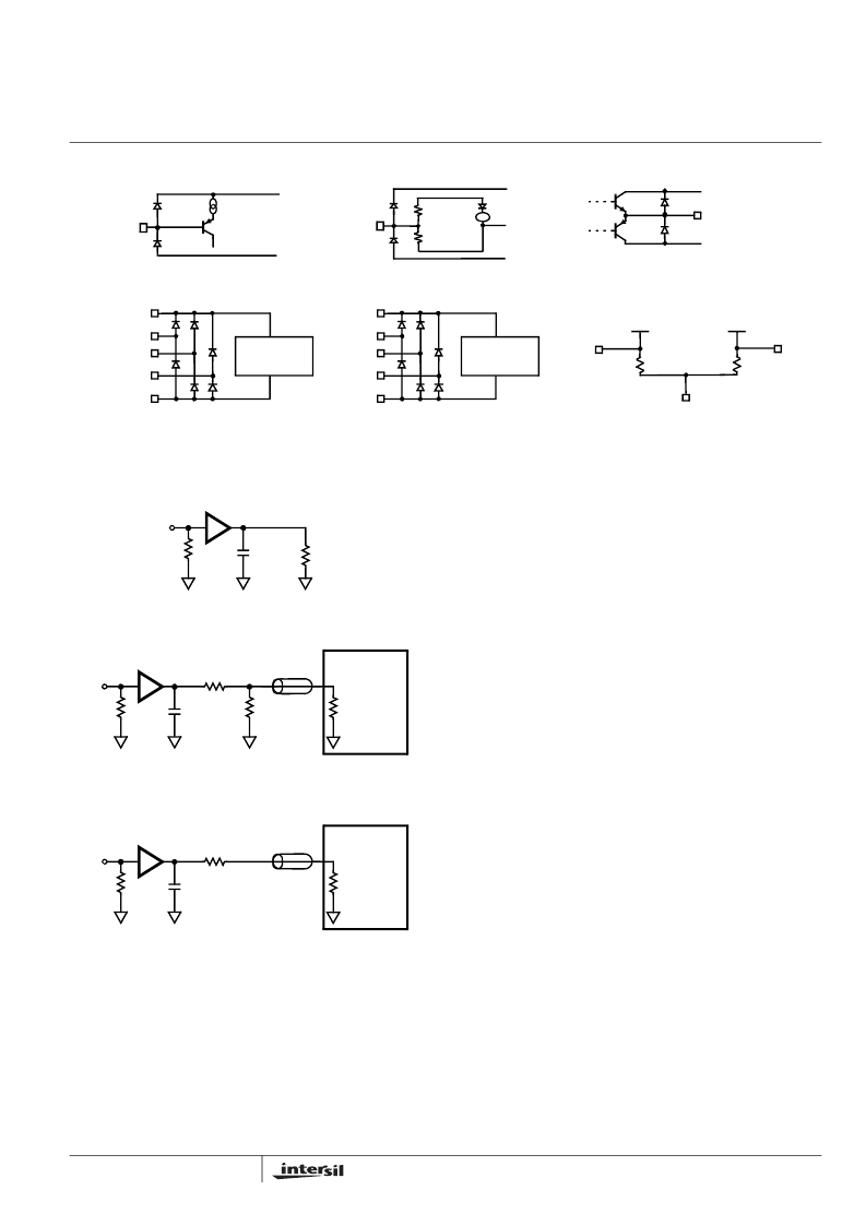
Pin Equivalent Circuits
Figure 42A illustrates the optimum output load for testing AC
performance. Figure 42B illustrates the optimum output load
when connecting to 50
Ω
input terminated equipment.
Application Information
General
The ISL59483 is ideal as the matrix element of high
performance switchers and routers. Key features include
high impedance buffered analog inputs and excellent AC
performance at output loads down to 150
Ω
for video cable-
driving. The current feedback output amplifiers are stable
operating into capacitive loads and bandwidth is optimized
with a load of 5pF in parallel with a 500
Ω
. Total output
capacitance can be split between the PCB capacitance and
an external load capacitor.
Ground Connections
For the best isolation and crosstalk rejection, all GND pins
must connect to the GND plane.
Power-up Considerations
The ESD protection circuits use internal diodes from all pins
the V+ and V- supplies. In addition, a dV/dT-triggered clamp
is connected between the V+ and V- pins, as shown in the
Equivalent Circuits 1 through 4 section of the Pin Description
table. The dV/dT triggered clamp imposes a maximum
supply turn-on slew rate of 1V/μs. Damaging currents can
flow for power supply rates-of-rise in excess of 1V/μs, such
as during hot plugging. Under these conditions, additional
methods should be employed to ensure the rate of rise is not
exceeded.
Consideration must be given to the order in which power is
applied to the V+ and V- pins, as well as analog and logic
input pins. Schottky diodes (Motorola MBR0550T or
equivalent) connected from V+ to ground and V- to ground
(Figure 43) will shunt damaging currents away from the
internal V+ and V- ESD diodes in the event that the V+
supply is applied to the device before the V- supply. One
Schottky can be used to protect both V+ power supply pins,
and a second for the protection of both V- pins.
IN
V+
V-
LOGIC PIN
V+
V-
GND
33k
21k
+
-
1.2V
V+
V-
OUT
CIRCUIT 3
CIRCUIT 2
CIRCUIT 1
V1-
~1M
Ω
SUBSTRATE 1
V1-
V1+
GNDB1
CAPACITIVELY
COUPLED
ESD CLAMP
GNDC1
GNDA1
V2-
V2+
GNDB2
CAPACITIVELY
COUPLED
ESD CLAMP
GNDC2
GNDA2
CIRCUIT 4B
CIRCUIT 4A
THERMAL HEAT SINK PAD
V2-
~1M
Ω
SUBSTRATE 2
AC Test Circuits
FIGURE 42A. TEST CIRCUIT WITH OPTIMAL OUTPUT LOAD
FIGURE 42B. TEST CIRCUIT FOR MEASURING WITH 50
Ω
OR
75
Ω
INPUT TERMINATED EQUIPMENT
FIGURE 42C. BACKLOADED TEST CIRCUIT FOR VIDEO
CABLE APPLICATION. BANDWIDTH AND
LINEARITY FOR R
L
LESS THAN 500
Ω
WILL BE
DEGRADED.
FIGURE 42. TEST CIRCUITS
ISL59483
C
L
5pF
50
Ω
or
75
Ω
V
IN
500
Ω
R
L
ISL59483
R
S
C
L
5pF
V
IN
475
Ω
TEST
50
Ω
or
75
Ω
50
Ω
or
75
Ω
50
Ω
or
75
Ω
EQUIPMENT
ISL59483
R
S
C
L
5pF
V
IN
50
Ω
or 75
Ω
TEST
50
Ω
or
75
Ω
50
Ω
or
75
Ω
EQUIPMENT
ISL59483
相关PDF资料 |
PDF描述 |
|---|---|
| ISL59483 | Dual, 500MHz Triple, Multiplexing Amplifiers |
| ISL59532IKEZ | 32x32 Video Crosspoint |
| ISL5957 | 14-Bit, +3.3V, 260+MSPS, High Speed D/A Converter |
| ISL5957IA | 14-Bit, +3.3V, 260+MSPS, High Speed D/A Converter |
| ISL5957IAZ | 14-Bit, +3.3V, 260+MSPS, High Speed D/A Converter |
相关代理商/技术参数 |
参数描述 |
|---|---|
| ISL59530 | 制造商:INTERSIL 制造商全称:Intersil Corporation 功能描述:16x16 Video Crosspoint |
| ISL59530_07 | 制造商:INTERSIL 制造商全称:Intersil Corporation 功能描述:16x16 Video Crosspoint |
| ISL59530_0708 | 制造商:INTERSIL 制造商全称:Intersil Corporation 功能描述:16x16 Video Crosspoint |
| ISL59530_11 | 制造商:INTERSIL 制造商全称:Intersil Corporation 功能描述:16x16 Video Crosspoint |
| ISL59530IKZ | 功能描述:IC CROSSPOINT SW 16X16 356PBGA RoHS:是 类别:集成电路 (IC) >> 接口 - 模拟开关,多路复用器,多路分解器 系列:- 应用说明:Ultrasound Imaging Systems Application Note 产品培训模块:Lead (SnPb) Finish for COTS Obsolescence Mitigation Program 标准包装:250 系列:- 功能:开关 电路:单刀单掷 导通状态电阻:48 欧姆 电压电源:单电源 电压 - 电源,单路/双路(±):2.7 V ~ 5.5 V 电流 - 电源:5µA 工作温度:0°C ~ 70°C 安装类型:表面贴装 封装/外壳:48-LQFP 供应商设备封装:48-LQFP(7x7) 包装:托盘 |
发布紧急采购,3分钟左右您将得到回复。