- 您现在的位置:买卖IC网 > PDF目录383137 > ISL59483IRZ-T13 (INTERSIL CORP) Dual, 500MHz Triple, Multiplexing Amplifiers PDF资料下载
参数资料
| 型号: | ISL59483IRZ-T13 |
| 厂商: | INTERSIL CORP |
| 元件分类: | 运动控制电子 |
| 英文描述: | Dual, 500MHz Triple, Multiplexing Amplifiers |
| 中文描述: | TRIPLE 2-CHANNEL, VIDEO MULTIPLEXER, PQCC48 |
| 封装: | 7 X 7 MM, ROHS COMPLIANT, PLASTIC, QFN-48 |
| 文件页数: | 14/17页 |
| 文件大小: | 909K |
| 代理商: | ISL59483IRZ-T13 |
14
FN6394.1
December 22, 2006
If positive voltages are applied to the logic or analog video
input pins before V+ is applied, current will flow through the
internal ESD diodes to the V+ pin. The presence of large
decoupling capacitors and the loading effect of other circuits
connected to V+ can result in damaging currents through the
ESD diodes and other active circuits within the device.
Therefore, adequate current limiting on the digital and
analog inputs is needed to prevent damage during the time
the voltages on these inputs are more positive than V+.
HIZ State
Each internal 4:1 triple MUX-amp has a high impedance
output control pin (HIZ1 and HIZ2). Each has an internal pull-
down resistor to set the output to the enabled state with no
connection to the HIZ pin. The HIZ state is established within
approximately 15ns by placing a logic high (>2V) on the HIZ
pin. If the HIZ state is selected, the MUX 1 output is a high
impedance 1.4M
Ω
with approximately 1.5pF in parallel with a
10
μ
A bias current from the output. In the HIZ state the MUX 2
output impedance is ~900
Ω
. The supply current during this
state is the same as the active state.
EN and Power-down States
The EN pin is active low. An internal pull-down resistor
ensures the device will be active with no connection to the
EN pin. The power-down state is established within
approximately 80ns if a logic high (>2V) is placed on the EN
pin. In the power-down state, supply current is reduced
significantly by shutting the three amplifiers off. The output
presents a high impedance to the output pin, however, there
is a risk that the disabled amplifier output can be back-driven
at signal voltage levels exceeding ~2V
P-P
. Under this
condition, large incoming slew rates can cause fault currents
of tens of mA
.
Therefore, the parallel connection of multiple
outputs is not recommended unless the application can
tolerate the limited power-down output impedance.
Output Capacitive Loading Considerations
High speed amplifiers may be sensitive to capacitance at the
output. Excessive pulse overshoot may result from the
combination of output slew rates approaching the amplifier
maximum and the presence of parasitic capacitance. In
applications where high slew rates are expected and PC board
output pin capacitance exceeds ~5pF, series connected
resistors (ranging from 10
Ω
to 75
Ω)
may be needed close to
the output pin in order to buffer the amplifer output stage from
the effects of capacitive loading. When paralleling the
amplifier outputs, resistance in series with MUX 1 output will
form a resistor divider with the 900
Ω
HIZ impedance of MUX 2
when MUX 1 is enabled and MUX 2 is in the HIZ state.
However, resistance in series with MUX 2 does not result in a
resistor divider with MUX 1 due to the 1.4M
Ω
HIZ impedance.
In all cases, series resistance will form a voltage divider with
any downstream load resistance, therefore the effects of
series resistance on throughput gain must be considered.
Limiting the Output Current
No output short circuit current limit exists on these parts. All
applications need to limit the output current to less than
50mA. Adequate thermal heat sinking of the parts is also
required.
PC Board Layout
The AC performance of this circuit depends greatly on the
care taken in designing the PC board. The following are
recommendations to achieve optimum high frequency
performance from your PC board.
The use of low inductance components such as chip
resistors and chip capacitors is strongly recommended.
Minimize signal trace lengths. Trace inductance and
capacitance can easily limit circuit performance. Avoid
sharp corners. Use rounded corners when possible. Vias
in the signal lines add inductance at high frequency and
should be avoided. PCB traces greater than 1" begin to
exhibit transmission line characteristics with signal rise/fall
times of 1ns or less. High frequency performance may be
degraded for traces greater than one inch, unless
controlled impedance (50
Ω
or 75
Ω
) strip lines or
microstrips are used.
Match channel to channel analog I/O trace lengths and
layout symmetry. This will minimize propagation delay
mismatches.
Maximize use of AC de-coupled PCB layers. All signal I/O
lines should be routed over continuous ground planes (i.e.
no split planes or PCB gaps under these lines). Avoid vias
in the signal I/O lines.
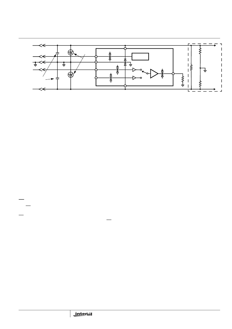
V+
V+
V-
V-
V+
V-
V+
V-
LOGIC
CONTROL
GND
IN0
IN1
S0
OUT
EXTERNAL
CIRCUITS
SCHOTTKY
PROTECTION
V+
V-
POWER
GND
SIGNAL
LOGIC
V+ SUPPLY
V- SUPPLY
DE-COUPLING
CAPS
FIGURE 43. SCHOTTKY PROTECTION CIRCUIT
ISL59483
相关PDF资料 |
PDF描述 |
|---|---|
| ISL59483 | Dual, 500MHz Triple, Multiplexing Amplifiers |
| ISL59532IKEZ | 32x32 Video Crosspoint |
| ISL5957 | 14-Bit, +3.3V, 260+MSPS, High Speed D/A Converter |
| ISL5957IA | 14-Bit, +3.3V, 260+MSPS, High Speed D/A Converter |
| ISL5957IAZ | 14-Bit, +3.3V, 260+MSPS, High Speed D/A Converter |
相关代理商/技术参数 |
参数描述 |
|---|---|
| ISL59530 | 制造商:INTERSIL 制造商全称:Intersil Corporation 功能描述:16x16 Video Crosspoint |
| ISL59530_07 | 制造商:INTERSIL 制造商全称:Intersil Corporation 功能描述:16x16 Video Crosspoint |
| ISL59530_0708 | 制造商:INTERSIL 制造商全称:Intersil Corporation 功能描述:16x16 Video Crosspoint |
| ISL59530_11 | 制造商:INTERSIL 制造商全称:Intersil Corporation 功能描述:16x16 Video Crosspoint |
| ISL59530IKZ | 功能描述:IC CROSSPOINT SW 16X16 356PBGA RoHS:是 类别:集成电路 (IC) >> 接口 - 模拟开关,多路复用器,多路分解器 系列:- 应用说明:Ultrasound Imaging Systems Application Note 产品培训模块:Lead (SnPb) Finish for COTS Obsolescence Mitigation Program 标准包装:250 系列:- 功能:开关 电路:单刀单掷 导通状态电阻:48 欧姆 电压电源:单电源 电压 - 电源,单路/双路(±):2.7 V ~ 5.5 V 电流 - 电源:5µA 工作温度:0°C ~ 70°C 安装类型:表面贴装 封装/外壳:48-LQFP 供应商设备封装:48-LQFP(7x7) 包装:托盘 |
发布紧急采购,3分钟左右您将得到回复。