参数资料
| 型号: | ISL5961IBZ |
| 厂商: | Intersil |
| 文件页数: | 2/13页 |
| 文件大小: | 0K |
| 描述: | CONV D/A 14-BIT 3.3V 28-SOIC |
| 标准包装: | 26 |
| 位数: | 14 |
| 数据接口: | 并联 |
| 转换器数目: | 1 |
| 电压电源: | 模拟和数字 |
| 功率耗散(最大): | 120mW |
| 工作温度: | -40°C ~ 85°C |
| 安装类型: | 表面贴装 |
| 封装/外壳: | 28-SOIC(0.295",7.50mm 宽) |
| 供应商设备封装: | 28-SOIC W |
| 包装: | 管件 |
| 输出数目和类型: | 2 电流,单极 |
| 采样率(每秒): | 150M |
10
Power Supply
Separate digital and analog power supplies are
recommended. The allowable supply range is +2.7V to
+3.6V. The recommended supply range is +3.0 to 3.6V
(nominally +3.3V) to maintain optimum SFDR. However,
operation down to +2.7V is possible with some degradation
in SFDR. Reducing the analog output current can help the
SFDR at +2.7V. The SFDR values stated in the table of
specifications were obtained with a +3.3V supply.
Ground Planes
Separate digital and analog ground planes should be used.
All of the digital functions of the device and their
corresponding components should be located over the
digital ground plane and terminated to the digital ground
plane. The same is true for the analog components and the
analog ground plane.
Noise Reduction
To minimize power supply noise, 0.1
F capacitors should be
placed as close as possible to the converter’s power supply
pins, AVDD and DVDD. Also, the layout should be designed
using separate digital and analog ground planes and these
capacitors should be terminated to the digital ground for
DVDD and to the analog ground for AVDD. Additional filtering
of the power supplies on the board is recommended.
Voltage Reference
The internal voltage reference of the device has a nominal
value of +1.23V with a
±40ppm/oC drift coefficient over the
full temperature range of the converter. It is recommended
that a 0.1
F capacitor be placed as close as possible to the
REFIO pin, connected to the analog ground. The REFLO pin
(16) selects the reference. The internal reference can be
selected if pin 16 is tied low (ground). If an external reference
is desired, then pin 16 should be tied high (the analog supply
voltage) and the external reference driven into REFIO, pin
17. The full scale output current of the converter is a function
of the voltage reference used and the value of RSET. IOUT
should be within the 2mA to 20mA range, though operation
below 2mA is possible, with performance degradation.
If the internal reference is used, VFSADJ will equal
approximately 1.2V (pin 18). If an external reference is used,
VFSADJ will equal the external reference. The calculation for
IOUT (Full Scale) is:
IOUT(Full Scale) = (VFSADJ/RSET) X 32.
If the full scale output current is set to 20mA by using the
internal voltage reference (1.2V) and a 1.91k
R
SET
resistor, then the input coding to output current will resemble
the following:
Analog Output
IOUTA and IOUTB are complementary current outputs. The
sum of the two currents is always equal to the full scale
output current minus one LSB. If single ended use is
desired, a load resistor can be used to convert the output
current to a voltage. It is recommended that the unused
output be either grounded or equally terminated. The voltage
developed at the output must not violate the output voltage
compliance range of -1.0V to 1.25V. ROUT (the impedance
loading each current output) should be chosen so that the
desired output voltage is produced in conjunction with the
output full scale current. If a known line impedance is to be
driven, then the output load resistor should be chosen to
match this impedance. The output voltage equation is:
VOUT = IOUT X ROUT.
The most effective method for reducing the power
consumption is to reduce the analog output current, which
dominates the supply current. The maximum recommended
output current is 20mA.
Differential Output
IOUTA and IOUTB can be used in a differential-to-single-
ended arrangement to achieve better harmonic rejection.
With RDIFF= 50 and RLOAD=50, the circuit in Figure 13
will provide a 500mV (-2.5dBm) signal at the output of the
transformer if the full scale output current of the DAC is set to
20mA (used for the electrical specifications table). Values of
RDIFF= 100 and RLOAD=50 were used for the typical
performance curves to increase the output power and the
dynamic range. The center tap in Figure 13 must be
grounded.
In the circuit in Figure 14, the user is left with the option to
ground or float the center tap. The DC voltage that will exist
at either IOUTA or IOUTB if the center tap is floating is
IOUTDC x (RA//RB) V because RDIFF is DC shorted by the
transformer. If the center tap is grounded, the DC voltage is
0V. Recommended values for the circuit in Figure 14 are
RA=RB=50, RDIFF=100, assuming RLOAD=50. The
performance of Figure 13 and Figure 14 is basically the
same, however leaving the center tap of Figure 14 floating
allows the circuit to find a more balanced virtual ground,
theoretically improving the even order harmonic rejection,
but likely reducing the signal swing available due to the
output voltage compliance range limitations.
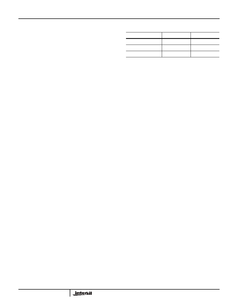
TABLE 1. INPUT CODING vs OUTPUT CURRENT WITH
INTERNAL REFERENCE AND RSET=1.91K
INPUT CODE (D13-D0)
IOUTA (mA)
IOUTB (mA)
1111 11111 11111
20
0
1000 00000 00000
10
0000 00000 00000
0
20
ISL5961
相关PDF资料 |
PDF描述 |
|---|---|
| ISL5961IAZ | CONV D/A 14-BIT 3.3V 28-TSSOP |
| 1-207825-4 | CONN RCPT CPC 4POS STD SER 1 PCB |
| ISL5861/2IAZ | CONV D/A 12-BIT HS 28-TSSOP |
| LT1190CS8#PBF | IC OP-AMP VIDEO HISPD SNGL 8SOIC |
| LT1190CS8 | IC OP-AMP VIDEO HISPD SNGL 8SOIC |
相关代理商/技术参数 |
参数描述 |
|---|---|
| ISL59830 | 制造商:INTERSIL 制造商全称:Intersil Corporation 功能描述:True Single Supply Video Driver |
| ISL59830_06 | 制造商:INTERSIL 制造商全称:Intersil Corporation 功能描述:True Single Supply Video Driver |
| ISL59830A | 制造商:INTERSIL 制造商全称:Intersil Corporation 功能描述:True Single Supply Video Driver With Power Down |
| ISL59830AIAZ | 功能描述:IC VIDEO DRIVER TRUE SGL 16-QSOP RoHS:是 类别:集成电路 (IC) >> 线性 - 放大器 - 视频放大器和频缓冲器 系列:- 产品培训模块:Lead (SnPb) Finish for COTS Obsolescence Mitigation Program 标准包装:50 系列:- 应用:TFT-LCD 面板:VCOM 驱动器 输出类型:满摆幅 电路数:1 -3db带宽:35MHz 转换速率:40 V/µs 电流 - 电源:3.7mA 电流 - 输出 / 通道:1.3A 电压 - 电源,单路/双路(±):9 V ~ 20 V,±4.5 V ~ 10 V 安装类型:表面贴装 封装/外壳:8-TSSOP,8-MSOP(0.118",3.00mm 宽)裸露焊盘 供应商设备封装:8-uMax-EP 包装:管件 |
| ISL59830AIAZ-T7 | 功能描述:IC VIDEO DRIVER TRUE SGL 16-QSOP RoHS:是 类别:集成电路 (IC) >> 线性 - 放大器 - 视频放大器和频缓冲器 系列:- 标准包装:1,000 系列:- 应用:驱动器 输出类型:差分 电路数:3 -3db带宽:350MHz 转换速率:1000 V/µs 电流 - 电源:14.5mA 电流 - 输出 / 通道:60mA 电压 - 电源,单路/双路(±):5 V ~ 12 V,±2.5 V ~ 6 V 安装类型:表面贴装 封装/外壳:20-VFQFN 裸露焊盘 供应商设备封装:20-QFN 裸露焊盘(4x4) 包装:带卷 (TR) |
发布紧急采购,3分钟左右您将得到回复。