- 您现在的位置:买卖IC网 > PDF目录20329 > ISL6144IRZA (Intersil)IC CTRLR O-RING MOSFET HV 20-QFN PDF资料下载
参数资料
| 型号: | ISL6144IRZA |
| 厂商: | Intersil |
| 文件页数: | 22/30页 |
| 文件大小: | 0K |
| 描述: | IC CTRLR O-RING MOSFET HV 20-QFN |
| 标准包装: | 60 |
| 应用: | 电信/数据通信系统 |
| FET 型: | N 沟道 |
| 输出数: | 1 |
| 内部开关: | 无 |
| 延迟时间 - 开启: | 1ms |
| 延迟时间 - 关闭: | 250ns |
| 电源电压: | 9 V ~ 75 V |
| 工作温度: | -40°C ~ 105°C |
| 安装类型: | 表面贴装 |
| 封装/外壳: | 20-VQFN 裸露焊盘 |
| 供应商设备封装: | 20-QFN 裸露焊盘(5x5) |
| 包装: | 管件 |
| 产品目录页面: | 1243 (CN2011-ZH PDF) |
第1页第2页第3页第4页第5页第6页第7页第8页第9页第10页第11页第12页第13页第14页第15页第16页第17页第18页第19页第20页第21页当前第22页第23页第24页第25页第26页第27页第28页第29页第30页
�� �
�
�ISL6144�
�P� loss� (� D1� )� =� P� loss� (� D2� )� =� ---------------� ?� V� F� =� 16A� ?� 0.5V� =� 8W�
�Fault� 6:� ORing� FET� Body� Diode� Conduction�
�(V� IN� -� 0.41V� >� V� OUT� ).� If� the� voltage� drop� across� the�
�MOSFET� approaches� 410mV,� a� fault� will� be� indicated.� Make�
�sure� the� selection� of� the� ORing� MOSFET� takes� this� fact� into�
�account.�
�Application� Considerations� and�
�Component� Selection�
�“ISL6144� +� ORing� FET”� vs� “ORing� Diode”� Solution�
�For� example,� in� a� 48V,� 32A� (1� +� 1)� redundant� system� with�
�current� sharing,� using� a� Schottky� diode� as� the� ORing� device�
�(Refer� to� Figure� 29),� the� forward� voltage� drop� is� in� the� 0.4V� to�
�0.7V� range,� (let� us� assume� it� is� 0.5V).� The� power� loss� across�
�each� diode� is� shown� in� Equation� 10:�
�I� OUT�
�2�
�(EQ.� 10)�
�The� total� power� loss� across� the� two� ORing� diodes� is� 16W.�
�“ISL6144� +� ORing� FET“� solution� is� more� efficient� than� the�
�“ORing� Diode”� Solution,� which� will� result� in� simplified� PCB�
�and� thermal� design.� It� will� also� eliminate� the� need� for� a� heat�
�sink� for� the� ORing� diode.� This� will� result� in� cost� savings.� In�
�addition� is� the� fact� that� the� ISL6144� solution� provides� a� more�
�flexible,� reliable� and� controllable� ORing� functionality� and�
�protects� against� system� fault� scenarios� (Refer� to� the� “Fault�
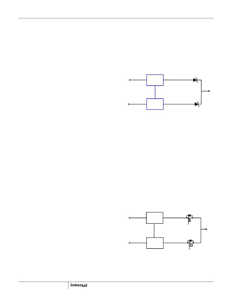
��INPUT� BUS� 1�
�INPUT� BUS� 2�
�DC/DC�
�1�
�CS�
�DC/DC�
�+IN1� =� 48V�
�+IN2� =� 48V�
�D� 1�
�0.5V@� 16A�
�D� 2�
�0.5V� @� 16A�
�V� OUT�
�(32A)�
�On� the� other� hand� the� most� common� failures� caused� by�
�diode� ORing� include� open� circuit� and� short� circuit� failures.� If�
�one� of� these� diodes� (Feed� A)� has� failed� open,� then� the� other�
�Feed� B� will� provide� all� of� the� power� demand.� The� system� will�
�continue� to� operate� without� any� notification� of� this� failure,�
�2�
�FIGURE� 29.� 1� +� 1� REDUNDANT� SYSTEM� WITH� DIODE� ORING�
�If� we� use� a� 4.5m� Ω� MOSFET� (refer� to� Figure� 30),� the� nominal�
�Power� loss� across� each� MOSFET� is:�
�P� loss� (� M� 1� )� =� P� loss� (� M� 2� )� =� ?� ---------------� ?� ?� r� DS� (� ON� )�
�P� loss� NOM� (� M� 1� )� =� (� 16A� )� ?� 4.5m� Ω� =� 1.152W�
�reducing� the� system� to� a� single� point� of� failure.� A� much� more�
�dangerous� failure� is� where� the� diode� has� failed� short.� The�
�system� will� continue� to� operate� without� notification� that� the�
�short� has� occurred.� With� this� failure,� transients� and� failures�
�2�
�?� 2� ?�
�I� OUT� 2�
�(EQ.� 11)�
�on� Feed� B� propagate� to� Feed� A.� Also,� this� silent� short� failure�
�could� pose� a� significant� safety� hazard� for� technical�
�personnel� servicing� these� feeds.�
�“ISL6144� +� ORing� FET”� vs� “Discrete� ORing� FET”�
�Solution�
�If� we� compare� the� ISL6144� integrated� solution� to� discrete�
�The� total� power� loss� across� the� two� ORing� MOSFETs� is�
�2.304W.�
�In� case� of� failure� of� current� sharing� scheme,� or� failure� of�
�DC/DC� 1,� the� full� load� will� be� supplied� by� DC/DC� 2.� ORing�
�MOSFET� M2� or� ORing� Diode� D� 2� will� be� conducting� the� full�
�load� current.� Power� lost� across� the� ORing� devices� are:�
�ORing� MOSFET� solutions� (with� similar� performance�
�parameters),� the� ISL6144� wins� in� all� aspects,� the� main� ones�
�P� loss� MAX� (� D� 2� )� =� I� OUT� ?� V� F� =� 32A� ?� 0.5V� =� 16W�
�(EQ.� 12)�
�P� loss� MAX� (� M2� )� =� (� I� OUT� )� ?� r� DS� (� ON� )� =� (� 32A� )� ?� 4.5m� Ω� =� 4.6W�
�being� simplicity� of� an� integrated� solution,� PCB� real� estate�
�saving,� cost� savings,� and� reduction� in� the� MTBF� of� this� section�
�of� the� circuit� as� the� overall� number� of� components� is� reduced.�
�2� 2�
�(EQ.� 13)�
�In� brief,� the� solution� offered� by� this� IC� enhances� power�
�system� performance� and� protection� while� not� adding� any�
�considerable� cost,� on� the� contrary� saving� PCB� board� real�
�estate� and� providing� a� simple� to� implement� integrated�
�INPUT� BUS� 1�
�DC/DC�
�1�
�+IN1� =� 48V�
�M1�
�4.5m� Ω�
�0.072V� @� 16A�
�solution.�
�ORing� MOSFET� Selection�
�Using� an� ORing� MOSFET� instead� of� an� ORing� diode� results�
�in� increased� overall� power� system� efficiency� as� losses� across�
�the� ORing� elements� are� reduced.� The� benefit� of� using� ORing�
�INPUT� BUS� 2�
�CS�
�DC/DC�
�2�
�+IN2� =� 48V�
�M2�
�4.5m� Ω�
�0.072V@� 16A�
�V� OUT�
�(32A)�
�MOSFETs� becomes� even� more� significant� at� higher� load�
�currents� as� power� loss� and� forward� voltage� drop� across� the�
�traditionally� used� ORing� diode� is� increased.� The� high� power�
�dissipation� across� these� diodes� requires� paralleling� of� many�
�diodes� as� well� as� special� thermal� design� precautions� such� as�
�heat� sinks� (heat� dissipating� pads)� and� forced� airflow.�
�22�
�FIGURE� 30.� 1+1� REDUNDANT� SYSTEM� WITH� MOSFET� ORING�
�FN9131.7�
�October� 6,� 2011�
�相关PDF资料 |
PDF描述 |
|---|---|
| ISL6146BFRZ-T7A | IC OR CTRLR N-CH 1CH 8DFN |
| B170B-13 | DIODE SCHOTTKY 70V 1A SMB |
| A470K15C0GL5UAA | CAP CER 47PF 500V 10% NP0 AXIAL |
| ISL6144IVZA-T | IC CTRLR MOSFET HV ORING 16TSSOP |
| EBM12DTAD-S189 | CONN EDGECARD 24POS R/A .156 SLD |
相关代理商/技术参数 |
参数描述 |
|---|---|
| ISL6144IRZA-T | 功能描述:IC CTRLR MOSFET HV ORING 20-QFN RoHS:是 类别:集成电路 (IC) >> PMIC - O 圈控制器 系列:- 标准包装:1,000 系列:- 应用:电池备份,工业/汽车,大电流开关 FET 型:- 输出数:5 内部开关:是 延迟时间 - 开启:100ns 延迟时间 - 关闭:- 电源电压:3 V ~ 5.5 V 电流 - 电源:250µA 工作温度:0°C ~ 70°C 安装类型:表面贴装 封装/外壳:16-SOIC(0.154",3.90mm 宽) 供应商设备封装:16-SOIC N 包装:带卷 (TR) |
| ISL6144IV | 功能描述:IC CTRLR MOSFET ORING HV 16TSSOP RoHS:否 类别:集成电路 (IC) >> PMIC - O 圈控制器 系列:- 标准包装:1,000 系列:- 应用:电池备份,工业/汽车,大电流开关 FET 型:- 输出数:5 内部开关:是 延迟时间 - 开启:100ns 延迟时间 - 关闭:- 电源电压:3 V ~ 5.5 V 电流 - 电源:250µA 工作温度:0°C ~ 70°C 安装类型:表面贴装 封装/外壳:16-SOIC(0.154",3.90mm 宽) 供应商设备封装:16-SOIC N 包装:带卷 (TR) |
| ISL6144IV-T | 功能描述:IC CTRLR MOSFET HV ORING 16TSSOP RoHS:否 类别:集成电路 (IC) >> PMIC - O 圈控制器 系列:- 标准包装:1,000 系列:- 应用:电池备份,工业/汽车,大电流开关 FET 型:- 输出数:5 内部开关:是 延迟时间 - 开启:100ns 延迟时间 - 关闭:- 电源电压:3 V ~ 5.5 V 电流 - 电源:250µA 工作温度:0°C ~ 70°C 安装类型:表面贴装 封装/外壳:16-SOIC(0.154",3.90mm 宽) 供应商设备封装:16-SOIC N 包装:带卷 (TR) |
| ISL6144IVZA | 功能描述:IC CTRLR MOSFET ORING HV 16TSSOP RoHS:是 类别:集成电路 (IC) >> PMIC - O 圈控制器 系列:- 标准包装:1,000 系列:- 应用:电池备份,工业/汽车,大电流开关 FET 型:- 输出数:5 内部开关:是 延迟时间 - 开启:100ns 延迟时间 - 关闭:- 电源电压:3 V ~ 5.5 V 电流 - 电源:250µA 工作温度:0°C ~ 70°C 安装类型:表面贴装 封装/外壳:16-SOIC(0.154",3.90mm 宽) 供应商设备封装:16-SOIC N 包装:带卷 (TR) |
| ISL6144IVZA-T | 功能描述:IC CTRLR MOSFET HV ORING 16TSSOP RoHS:是 类别:集成电路 (IC) >> PMIC - O 圈控制器 系列:- 标准包装:1,000 系列:- 应用:电池备份,工业/汽车,大电流开关 FET 型:- 输出数:5 内部开关:是 延迟时间 - 开启:100ns 延迟时间 - 关闭:- 电源电压:3 V ~ 5.5 V 电流 - 电源:250µA 工作温度:0°C ~ 70°C 安装类型:表面贴装 封装/外壳:16-SOIC(0.154",3.90mm 宽) 供应商设备封装:16-SOIC N 包装:带卷 (TR) |
发布紧急采购,3分钟左右您将得到回复。