- 您现在的位置:买卖IC网 > PDF目录176104 > ISL6227 (Intersil Corporation) Dual Mobile-Friendly PWM Controller with DDR Option PDF资料下载
参数资料
| 型号: | ISL6227 |
| 厂商: | Intersil Corporation |
| 英文描述: | Dual Mobile-Friendly PWM Controller with DDR Option |
| 中文描述: | 双移动友好PWM控制器与DDR选项 |
| 文件页数: | 1/26页 |
| 文件大小: | 897K |
| 代理商: | ISL6227 |
1
ISL6227
Dual Mobile-Friendly PWM Controller with
DDR Option
The ISL6227 dual PWM controller delivers high efficiency
precision voltage regulation from two synchronous buck DC/DC
converters. It was designed especially to provide power
regulation for DDR memory, chipsets, graphics and other
system electronics in Notebook PCs. The ISL6227’s wide
input voltage range capability allows for voltage conversion
directly from ac/dc adaptor or Li-Ion battery pack.
Automatic mode transition of constant-frequency synchronous
rectification at heavy load, and hysteretic (HYS) diode-
emulation at light load, assure high efficiency over a wide range
of conditions. The HYS mode of operation can be disabled
separately on each PWM converter if constant-frequency
continuous-conduction operation is desired for all load levels.
Efficiency is further enhanced by using the lower MOSFET
rDS(ON) as the current sense element.
Voltage-feed-forward ramp modulation, current mode control,
and internal feedback compensation provide fast response to
input voltage and load transients. Input current ripple is
minimized by channel-to-channel PWM phase shift of 0°, 90°, or
180° (determined by input voltage and status of the DDR pin).
The ISL6227 can control two independent output voltages
adjustable from 0.9V to 5.5V, or by activating the DDR pin,
transform into a complete DDR memory power supply solution.
In DDR mode, CH2 output voltage VTT tracks CH1 output
voltage VDDQ. CH2 output can both source and sink current, an
essential power supply feature for DDR memory. The reference
voltage VREF required by DDR memory is generated as well.
In dual power supply applications the ISL6227 monitors the
output voltage of both CH1 and CH2. An independent PGOOD
(power good) signal is asserted for each channel after the soft-
start sequence has completed, and the output voltage is within
PGOOD window. In DDR mode CH1 generates the only
PGOOD signal.
Built-in overvoltage protection prevents the output from going
above 115% of the set point by holding the lower MOSFET on
and the upper MOSFET off. When the output voltage re-enters
regulation, PGOOD will go HIGH and normal operation
automatically resumes. Once the soft-start sequence has
completed, undervoltage protection latches the offending
channel off if the output drops below 75% of its set point value.
Adjustable overcurrent protection (OCP) monitors the voltage
drop across the rDS(ON) of the lower MOSFET. If more precise
current-sensing is required, an external current sense resistor
may be used.
Applications
Notebook PCs and Desknotes
Tablet PCs/Slates
Hand-held portable instruments
Features
Provides regulated output voltage in the range 0.9V–5.5V
Operates from an input battery voltage range of 5V to 24V
or from 3.3V/5V system rail
Complete DDR1 and DDR2 memory power solution with
VTT tracking VDDQ/2 and a VDDQ/2 buffered reference
output
Flexible PWM or HYS plus PWM mode selection with HYS
diode emulation at light loads for higher system efficiency
rDS(ON) current sensing
Excellent dynamic response with voltage feed-forward and
current mode control accommodating wide range LC filter
selections
Undervoltage lock-out on VCC pin
Power-good, overcurrent, overvoltage, undervoltage
protection for both channels
Synchronized 300kHz PWM operation in PWM mode
Pb-Free Available as an Option
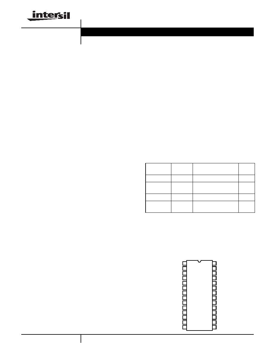
Pinout
ISL6227 (28 LD SSOP)
TOP VIEW
Ordering Information
PART #
TEMP. (°C)
PACKAGE
PKG.
DWG. #
ISL6227CA
-10 to 100 28 Ld SSOP
M28.15
ISL6227CAZ
(Note)
-10 to 100 28 Ld SSOP (Pb-Free)
M28.15
ISL6227CA-T
-10 to 100 28 Ld SSOP Tape and Reel M28.15
ISL6227CAZ-T
(Note)
-10 to 100 28 Ld SSOP Tape and Reel
(Pb-Free)
M28.15
NOTE: Intersil Pb-Free products employ special Pb-free material
sets; molding compounds/die attach materials and 100% matte tin
plate termination finish, which is compatible with both SnPb and
Pb-free soldering operations. Intersil Pb-Free products are MSL
classified at Pb-free peak reflow temperatures that meet or exceed
the Pb-free requirements of IPC/JEDEC J Std-020B.
EN1
GND
DDR
VSEN1
VIN
PG1
VCC
VOUT1
ISEN1
LGATE1
PGND1
BOOT1
UGATE1
PHASE1
ISEN2
LGATE2
PGND2
BOOT2
UGATE2
PHASE2
EN2
VSEN2
VOUT2
OCSET2
OCSET1
SOFT1
SOFT2
PG2/REF
28
27
26
25
24
23
22
21
20
19
18
17
16
15
1
2
3
4
5
6
7
8
9
10
11
12
13
14
March 2004
Data Sheet
FN9094.1
相关PDF资料 |
PDF描述 |
|---|---|
| ISL6292DCRZ-T | Li-ion/Li Polymer Battery Charger |
| ISL6537ACR | ACPI Regulator/Controller for Dual Channel DDR Memory Systems |
| ISL6537A | ACPI Regulator/Controller for Dual Channel DDR Memory Systems |
| ISL6612BIRZ-T | Advanced Synchronous Rectified Buck MOSFET Drivers with Pre-POR OVP |
| ISL6613BIRZ-T | Advanced Synchronous Rectified Buck MOSFET Drivers with Pre-POR OVP |
相关代理商/技术参数 |
参数描述 |
|---|---|
| ISL6227_07 | 制造商:INTERSIL 制造商全称:Intersil Corporation 功能描述:Dual Mobile-Friendly PWM Controller with DDR Option |
| ISL6227CA | 功能描述:IC CONTROLLER DDR, DDR2 28QSOP RoHS:否 类别:集成电路 (IC) >> PMIC - 稳压器 - 专用型 系列:- 产品培训模块:Lead (SnPb) Finish for COTS Obsolescence Mitigation Program 标准包装:2,000 系列:- 应用:电源,ICERA E400,E450 输入电压:4.1 V ~ 5.5 V 输出数:10 输出电压:可编程 工作温度:-40°C ~ 85°C 安装类型:表面贴装 封装/外壳:42-WFBGA,WLCSP 供应商设备封装:42-WLP 包装:带卷 (TR) |
| ISL6227CA-T | 功能描述:IC CONTROLLER DDR, DDR2 28QSOP RoHS:否 类别:集成电路 (IC) >> PMIC - 稳压器 - 专用型 系列:- 产品培训模块:Lead (SnPb) Finish for COTS Obsolescence Mitigation Program 标准包装:2,000 系列:- 应用:电源,ICERA E400,E450 输入电压:4.1 V ~ 5.5 V 输出数:10 输出电压:可编程 工作温度:-40°C ~ 85°C 安装类型:表面贴装 封装/外壳:42-WFBGA,WLCSP 供应商设备封装:42-WLP 包装:带卷 (TR) |
| ISL6227CAZ | 功能描述:电流型 PWM 控制器 VER OF ISL6227CA RoHS:否 制造商:Texas Instruments 开关频率:27 KHz 上升时间: 下降时间: 工作电源电压:6 V to 15 V 工作电源电流:1.5 mA 输出端数量:1 最大工作温度:+ 105 C 安装风格:SMD/SMT 封装 / 箱体:TSSOP-14 |
| ISL6227CAZS2698 | 功能描述:IC CONTROLLER DDR, DDR2 28QSOP RoHS:是 类别:集成电路 (IC) >> PMIC - 稳压器 - 专用型 系列:- 标准包装:43 系列:- 应用:控制器,Intel VR11 输入电压:5 V ~ 12 V 输出数:1 输出电压:0.5 V ~ 1.6 V 工作温度:-40°C ~ 85°C 安装类型:表面贴装 封装/外壳:48-VFQFN 裸露焊盘 供应商设备封装:48-QFN(7x7) 包装:管件 |
发布紧急采购,3分钟左右您将得到回复。