- 您现在的位置:买卖IC网 > Datasheet目录333 > ISL6261AEVAL1Z (Intersil)EVAL BOARD 1 FOR ISL6261A Datasheet资料下载
参数资料
| 型号: | ISL6261AEVAL1Z |
| 厂商: | Intersil |
| 文件页数: | 21/34页 |
| 文件大小: | 0K |
| 描述: | EVAL BOARD 1 FOR ISL6261A |
| 标准包装: | 1 |
| 系列: | * |
第1页第2页第3页第4页第5页第6页第7页第8页第9页第10页第11页第12页第13页第14页第15页第16页第17页第18页第19页第20页当前第21页第22页第23页第24页第25页第26页第27页第28页第29页第30页第31页第32页第33页第34页
�� �
�
�ISL6261A�
�After� determining� R� s� and� R� n� networks,� use� Equation� 23� to�
�calculate� the� droop� resistances� R� drp1� and� R� drp2� .�
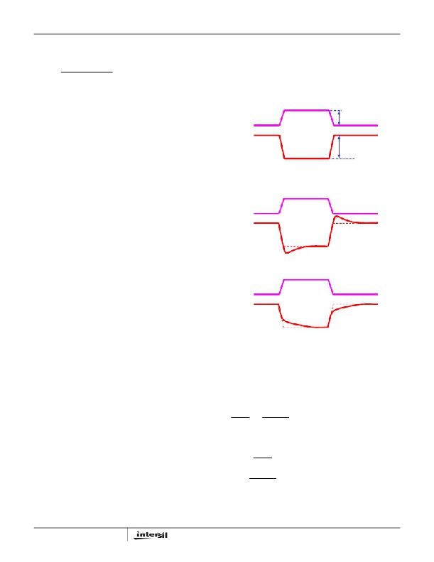
�response.� Figure� 11� shows� the� transient� response� when� C� n�
�is� too� small.� V� core� may� sag� excessively� upon� load�
�R� drp� 2� =� (�
�R� droop�
�DCR� ?� G� 1� (� 25� o� C� )�
�?� 1� )� ?� R� drp� 1�
�(EQ.� 23)�
�application� to� create� a� system� failure.� Figure� 12� shows� the�
�transient� response� when� C� n� is� too� large.� V� core� is� sluggish� in�
�drooping� to� its� final� value.� There� will� be� excessive� overshoot�
�R� droop� is� 2.1mV/A� per� lntel� ?� IMVP-6� ?� specification.�
�The� effectiveness� of� the� R� n� network� is� sensitive� to� the�
�if� a� load� occurs� during� this� time,� which� may� potentially� hurt�
�the� CPU� reliability.�
�coupling� coefficient� between� the� NTC� thermistor� and� the�
�inductor.� The� NTC� thermistor� should� be� placed� in� close�
�proximity� of� the� inductor.�
�i� core�
�Δ� I� core�
�To� verify� whether� the� NTC� network� successfully� compensates�
�the� DCR� change� over� temperature,� one� can� apply� full� load�
�V� core�
�V� core�
�Δ� V� core�
�current,� wait� for� the� thermal� steady� state,� and� see� how� much�
�the� output� voltage� deviates� from� the� initial� voltage� reading.�
�Good� thermal� compensation� can� limit� the� drift� to� less� than�
�2mV.� If� the� output� voltage� decreases� when� the� temperature�
�increases,� that� ratio� between� the� NTC� thermistor� value� and�
�the� rest� of� the� resistor� divider� network� has� to� be� increased.�
�Following� the� evaluation� board� value� and� layout� of� NTC�
�placement� will� minimize� the� engineering� time.�
�Δ� V� core� =� Δ� I� core� ×� R� droop�
�FIGURE� 10.� DESIRED� LOAD� TRANSIENT� RESPONSE�
�WAVEFORMS�
�i� core�
�The� current� sensing� traces� should� be� routed� directly� to� the�
�inductor� pads� for� accurate� DCR� voltage� drop� measurement.�
�However,� due� to� layout� imperfection,� the� calculated� R� drp2�
�V� core�
�V� core�
�R� drp� 2� _� new� =�
�(� R� drp� 1� +� R� drp� 2� )� ?� R� drp� 1�
�?� ?� � C� n�
�=� ?� ?� n�
�may� still� need� slight� adjustment� to� achieve� optimum� load� line�
�slope.� It� is� recommended� to� adjust� R� drp2� after� the� system�
�has� achieved� thermal� equilibrium� at� full� load.� For� example,� if�
�the� max� current� is� 20A,� one� should� apply� 20A� load� current�
�and� look� for� 42mV� output� voltage� droop.� If� the� voltage� droop�
�is� 40mV,� the� new� value� of� R� dpr2� is� calculated� by:�
�42� mV�
�40� mV�
�(EQ.� 24)�
�For� the� best� accuracy,� the� effective� resistance� on� the� DFB�
�and� VSUM� pins� should� be� identical� so� that� the� bias� current�
�of� the� droop� amplifier� does� not� cause� an� offset� voltage.� The�
�effective� resistance� on� the� VSUM� pin� is� the� parallel� of� R� s� and�
�R� n� ,� and� the� effective� resistance� on� the� DFB� pin� is� the� parallel�
�of� R� drp1� and� R� drp2� .�
�Dynamic� Mode� of� Operation� –� Droop� Capacitor�
�Design� in� DCR� Sensing�
�Figure� 10� shows� the� desired� waveforms� during� load�
�transient� response.� V� core� needs� to� be� as� square� as� possible�
�at� I� core� change.� The� V� core� response� is� determined� by� several�
�factors,� namely� the� choice� of� output� inductor� and� output�
�capacitor,� the� compensator� design,� and� the� droop� capacitor�
�FIGURE� 11.� LOAD� TRANSIENT� RESPONSE� WHEN� C� n� IS� TOO�
�SMALL�
�i� core�
�V� core� V� core�
�FIGURE� 12.� LOAD� TRANSIENT� RESPONSE� WHEN� C� n� IS� TOO�
�LARGE�
�The� current� sensing� network� consists� of� R� n� ,� R� s� and� C� n� .� The�
�effective� resistance� is� the� parallel� of� R� n� and� R� s� .� The� RC� time�
�constant� of� the� current� sensing� network� needs� to� match� the�
�L/DCR� time� constant� of� the� inductor� to� get� correct�
�representation� of� the� inductor� current� waveform.� Equation� 25�
�shows� this� equation:�
�L� ?� R� � R� s� ?� (EQ.� 25)�
�DCR� ?� R� n� +� R� s� ?�
�Solving� for� Cn� yields:�
�L�
�C� n� =� DCR�
�design.�
�The� droop� capacitor� refers� to� C� n� in� Figure� 9.� If� C� n� is�
�designed� correctly,� its� voltage� will� be� a� high-bandwidth�
�analog� voltage� of� the� inductor� current.� If� C� n� is� not� designed�
�correctly,� its� voltage� will� be� distorted� from� the� actual�
�waveform� of� the� inductor� current� and� worsen� the� transient�
�21�
�R� n� � R� s�
�R� n� +� R� s�
�(EQ.� 26)�
�FN6354.3�
�November� 5,� 2009�
�相关PDF资料 |
PDF描述 |
|---|---|
| ISL6261EVAL1Z | EVAL BOARD FOR ISL6261 1 QFN |
| ISL6271AEVAL1 | EVALUATION BOARD FOR ISL6271A |
| ISL62882CEVAL2Z | EVAL BOARD FOR ISL62882C |
| ISL62883CEVAL2Z | EVAL BOARD FOR ISL62883C |
| ISL62883EVAL2Z | EVALUATION BOARD FOR ISL62883 |
相关代理商/技术参数 |
参数描述 |
|---|---|
| ISL6261AEVAL2Z | 功能描述:EVAL BOARD 2 FOR ISL6261A RoHS:是 类别:编程器,开发系统 >> 评估板 - 线性稳压器 (LDO) 系列:* 产品变化通告:1Q2012 Discontinuation 30/Mar/2012 设计资源:NCP590MNDPTAGEVB Gerber Files 标准包装:1 系列:- 每 IC 通道数:2 - 双 输出电压:1.8V,2.8V 电流 - 输出:300mA 输入电压:2.1 ~ 5.5 V 稳压器类型:正,固定式 工作温度:-40°C ~ 85°C 板类型:完全填充 已供物品:板 已用 IC / 零件:NCP590MNDP 其它名称:NCP590MNDPTAGEVB-NDNCP590MNDPTAGEVBOS |
| ISL6261AIRZ | 功能描述:DC/DC 开关控制器 ONE-PHS INT DC/DC BUCK CNTRLR IMVP-6 RoHS:否 制造商:Texas Instruments 输入电压:6 V to 100 V 开关频率: 输出电压:1.215 V to 80 V 输出电流:3.5 A 输出端数量:1 最大工作温度:+ 125 C 安装风格: 封装 / 箱体:CPAK |
| ISL6261AIRZ-T | 功能描述:DC/DC 开关控制器 ONE-PHS INT DC/DC BUCK CNTRLR IMVP-6 RoHS:否 制造商:Texas Instruments 输入电压:6 V to 100 V 开关频率: 输出电压:1.215 V to 80 V 输出电流:3.5 A 输出端数量:1 最大工作温度:+ 125 C 安装风格: 封装 / 箱体:CPAK |
| ISL6261CR7Z | 功能描述:IC CTRLR BUCK 1PHASE 48-VFQFN EP RoHS:是 类别:集成电路 (IC) >> PMIC - 稳压器 - 专用型 系列:- 标准包装:43 系列:- 应用:控制器,Intel VR11 输入电压:5 V ~ 12 V 输出数:1 输出电压:0.5 V ~ 1.6 V 工作温度:-40°C ~ 85°C 安装类型:表面贴装 封装/外壳:48-VFQFN 裸露焊盘 供应商设备封装:48-QFN(7x7) 包装:管件 |
| ISL6261CR7Z-T | 功能描述:IC CTRLR BUCK 1PHASE 48-VFQFN-EP RoHS:是 类别:集成电路 (IC) >> PMIC - 稳压器 - 专用型 系列:- 标准包装:43 系列:- 应用:控制器,Intel VR11 输入电压:5 V ~ 12 V 输出数:1 输出电压:0.5 V ~ 1.6 V 工作温度:-40°C ~ 85°C 安装类型:表面贴装 封装/外壳:48-VFQFN 裸露焊盘 供应商设备封装:48-QFN(7x7) 包装:管件 |
发布紧急采购,3分钟左右您将得到回复。