参数资料
| 型号: | ISL6263BHRZ-T |
| 厂商: | Intersil |
| 文件页数: | 17/18页 |
| 文件大小: | 0K |
| 描述: | IC DC/DC BUCK CTRLR 1PH 32-QFN |
| 标准包装: | 6,000 |
| 应用: | 转换器,Intel IMVP-6 |
| 输入电压: | 5 V ~ 25 V |
| 输出数: | 1 |
| 输出电压: | 0.41 V ~ 1.29 V |
| 工作温度: | -10°C ~ 100°C |
| 安装类型: | 表面贴装 |
| 封装/外壳: | 32-VFQFN 裸露焊盘 |
| 供应商设备封装: | 32-QFN(5x5) |
| 包装: | 带卷 (TR) |
�� �
�
�ISL6263B�
�LGATE,� PVCC,� and� PGND�
�PGND� is� the� return� path� for� the� pull-down� of� the� LGATE�
�low-side� MOSFET� gate� driver.� Ideally,� PGND� should� be�
�connected� to� the� source� of� the� low-side� MOSFET� with� a�
�low-resistance,� low-inductance� path.� The� LGATE� trace� should�
�be� routed� in� parallel� with� the� trace� from� the� PGND� pin.� These�
�two� traces� should� be� short,� wide,� and� away� from� other� traces�
�because� of� the� high� peak� current� and� extremely� fast� dv/dt.�
�PVCC� should� be� decoupled� to� PGND� with� a� ceramic�
�capacitor� physically� located� as� close� as� practical� to� the� IC�
�pins.�
�RBIAS�
�The� resistor� R� RBIAS� should� be� placed� in� close� proximity� to�
�the� ISL6263B� using� a� noise-free� current� return� path� to� the�
�VSS� pin.�
�IMON,� SOFT,� OCSET,� V� W,� COMP,� FB,� VDIFF,�
�DROOP,� DFB,� VO,� and� VSUM�
�The� traces� and� components� associated� with� these� pins�
�require� close� proximity� to� the� IC� as� well� as� close� proximity� to�
�each� other.� This� section� of� the� converter� circuit� needs� to� be�
�located� above� the� island� of� analog� ground� with� the�
�single-point� connection� to� the� VSS� pin.�
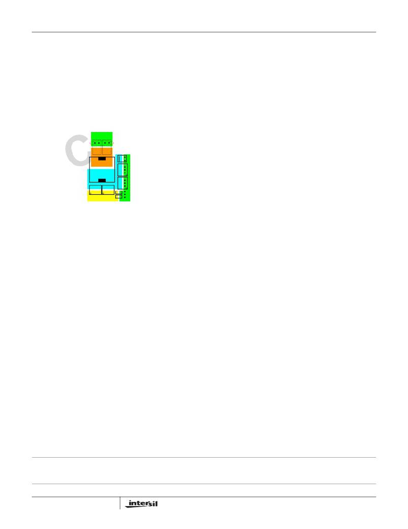
�VIAS� TO�
�GROUND�
�PLANE�
�INDUCTOR�
�HIGH-SIDE�
�MOSFETS�
�GND�
�VOUT�
�PHASE�
�NODE�
�VIN�
�OUTPUT�
�CAPACITORS�
�SCHOTTKY�
�DIODE�
�LOW-SIDE�
�MOSFETS�
�INPUT�
�CAPACITORS�
�Resistor� R� S�
�Resistor� R� S� is� preferably� located� near� the� boundary�
�between� the� power� ground� and� the� island� of� analog� ground�
�connected� to� the� VSS� pin.�
�VID<0:4>,� AF_EN,� PGOOD,� and� VR_ON�
�These� are� logic� signals� that� do� not� require� special� attention.�
�FDE�
�FIGURE� 13.� TYPICAL� POWER� COMPONENT� PLACEMENT�
�UGATE,� BOOT,� and� PHASE�
�PHASE� is� the� return� path� for� the� entire� UGATE� high-side�
�MOSFET� gate� driver.� The� layout� for� these� signals� require�
�similar� treatment,� but� to� a� greater� extent,� than� those� for�
�LGATE,� PVCC,� and� PGND.� These� signals� swing� from�
�approximately� VIN� to� VSS� and� are� more� likely� to� couple� into�
�other� signals.�
�VSEN� and� RTN�
�These� traces� should� be� laid� out� as� noise� sensitive.� For�
�optimum� load� line� regulation� performance,� the� traces�
�connecting� these� two� pins� to� the� Kelvin� sense� leads� of� the�
�processor� should� be� laid� out� away� from� rapidly� rising� voltage�
�nodes,� (switching� nodes)� and� other� noisy� traces.� The� filter�
�capacitors� C� FILTER1� ,� C� FILTER2� ,� and� C� FILTER3� used� in�
�conjunction� with� filter� resistors� R� FILTER1� and� R� FILTER2� form�
�common� mode� and� differential� mode� filters� as� shown� in�
�This� logic� signal� should� be� treated� as� noise� sensitive� and�
�should� be� routed� away� from� rapidly� rising� voltage� nodes,�
�(switching� nodes)� and� other� noisy� traces.�
�VIN�
�The� VIN� signal� should� be� connected� near� the� drain� of� the�
�high-side� MOSFET.�
�Copper� Size� for� the� Phase� Node�
�The� parasitic� capacitance� and� parasitic� inductance� of� the�
�phase� node� should� be� kept� very� low� to� minimize� ringing.� It� is�
�best� to� limit� the� size� of� the� PHASE� node� copper� in� strict�
�accordance� with� the� current� and� thermal� management� of� the�
�application.� An� MLCC� should� be� connected� directly� across�
�the� drain� of� the� high-side� MOSFET� and� the� source� of� the�
�low-side� MOSFET� to� suppress� turn-off� voltage� spikes.�
�Figure� 8.� The� noise� environment� of� the� application� and�
�actual� board� layout� conditions� will� drive� the� extent� of� filter�
�complexity.� The� maximum� recommended� resistance� for�
�R� FILTER1� and� R� FILTER2� is� approximately� 10� Ω� to� avoid�
�interaction� with� the� 50k� Ω� input� resistance� of� the� remote�
�sense� differential� amplifier.� The� physical� location� of� these�
�resistors� is� not� as� critical� as� the� filter� capacitors.� Typical�
�capacitance� values� for� C� FILTER1� ,� C� FILTER2� ,� and� C� FILTER3�
�range� between� 330pF� to� 1000pF� and� should� be� placed� near�
�the� IC.�
�All� Intersil� U.S.� products� are� manufactured,� assembled� and� tested� utilizing� ISO9000� quality� systems.�
�Intersil� Corporation’s� quality� certifications� can� be� viewed� at� www.intersil.com/design/quality�
�Intersil� products� are� sold� by� description� only.� Intersil� Corporation� reserves� the� right� to� make� changes� in� circuit� design,� software� and/or� specifications� at� any� time� without�
�notice.� Accordingly,� the� reader� is� cautioned� to� verify� that� data� sheets� are� current� before� placing� orders.� Information� furnished� by� Intersil� is� believed� to� be� accurate� and�
�reliable.� However,� no� responsibility� is� assumed� by� Intersil� or� its� subsidiaries� for� its� use;� nor� for� any� infringements� of� patents� or� other� rights� of� third� parties� which� may� result�
�from� its� use.� No� license� is� granted� by� implication� or� otherwise� under� any� patent� or� patent� rights� of� Intersil� or� its� subsidiaries.�
�For� information� regarding� Intersil� Corporation� and� its� products,� see� www.intersil.com�
�17�
�FN6388.3�
�July� 8,� 2010�
�相关PDF资料 |
PDF描述 |
|---|---|
| X40030V14-A | IC VOLTAGE MONITOR TRPL 14-TSSOP |
| ISL6262CRZ-T | IC CORE REG 2PHASE 48-QFN |
| X40030S14I-CT1 | IC VOLTAGE MONITOR TRPL 14-SOIC |
| ASC25DREN-S13 | CONN EDGECARD 50POS .100 EXTEND |
| X40030S14I-C | IC VOLTAGE MONITOR TRPL 14-SOIC |
相关代理商/技术参数 |
参数描述 |
|---|---|
| ISL6263C | 制造商:INTERSIL 制造商全称:Intersil Corporation 功能描述:5-Bit VID Single-Phase Voltage Regulator with Current Monitor for GPU Core Power |
| ISL6263CEVAL1 | 功能描述:EVAL BOARD 1 FOR ISL6263C RoHS:否 类别:编程器,开发系统 >> 评估板 - 线性稳压器 (LDO) 系列:* 产品变化通告:1Q2012 Discontinuation 30/Mar/2012 设计资源:NCP590MNDPTAGEVB Gerber Files 标准包装:1 系列:- 每 IC 通道数:2 - 双 输出电压:1.8V,2.8V 电流 - 输出:300mA 输入电压:2.1 ~ 5.5 V 稳压器类型:正,固定式 工作温度:-40°C ~ 85°C 板类型:完全填充 已供物品:板 已用 IC / 零件:NCP590MNDP 其它名称:NCP590MNDPTAGEVB-NDNCP590MNDPTAGEVBOS |
| ISL6263CHRZ | 功能描述:直流/直流开关调节器 1-PHS INT DC/DC BUCK CNTRLR IMVP-6 W/IMON RoHS:否 制造商:International Rectifier 最大输入电压:21 V 开关频率:1.5 MHz 输出电压:0.5 V to 0.86 V 输出电流:4 A 输出端数量: 最大工作温度: 安装风格:SMD/SMT 封装 / 箱体:PQFN 4 x 5 |
| ISL6263CHRZ-T | 功能描述:直流/直流开关调节器 1-PHS INT DC/DC BUCK CNTRLR IMVP-6 W/IMON RoHS:否 制造商:International Rectifier 最大输入电压:21 V 开关频率:1.5 MHz 输出电压:0.5 V to 0.86 V 输出电流:4 A 输出端数量: 最大工作温度: 安装风格:SMD/SMT 封装 / 箱体:PQFN 4 x 5 |
| ISL6263CRZ | 功能描述:直流/直流开关调节器 1 PHS INT DC/DC BUCK CNTRLR FOR INTEL RoHS:否 制造商:International Rectifier 最大输入电压:21 V 开关频率:1.5 MHz 输出电压:0.5 V to 0.86 V 输出电流:4 A 输出端数量: 最大工作温度: 安装风格:SMD/SMT 封装 / 箱体:PQFN 4 x 5 |
发布紧急采购,3分钟左右您将得到回复。