参数资料
| 型号: | ISL6315IRZ |
| 厂商: | Intersil |
| 文件页数: | 14/20页 |
| 文件大小: | 0K |
| 描述: | IC REG CTRLR BUCK PWM VM 24-QFN |
| 标准包装: | 75 |
| PWM 型: | 电压模式 |
| 输出数: | 1 |
| 频率 - 最大: | 255kHz |
| 占空比: | 67% |
| 电源电压: | 4.75 V ~ 5.25 V |
| 降压: | 是 |
| 升压: | 无 |
| 回扫: | 无 |
| 反相: | 无 |
| 倍增器: | 无 |
| 除法器: | 无 |
| Cuk: | 无 |
| 隔离: | 无 |
| 工作温度: | -40°C ~ 85°C |
| 封装/外壳: | 24-VFQFN 裸露焊盘 |
| 包装: | 管件 |
�� �
�
�ISL6315�
�and� E� represents� the� total� output� capacitance� and� its�
�equivalent� series� resistance.�
�frequency� response� of� the� modulator� (G� MOD� ),� feedback�
�compensation� (G� FB� )� and� closed-loop� response� (G� CL� ):�
�F� LC� =� ---------------------------�
�F� CE� =� ------------------------�
�G� MOD� (� f� )� =� ------------------------------� ?� ----------------------------------------------------------------------------------------�
�V� OSC�
�1� +� s� (� f� )� ?� (� E� +� D� )� ?� C� +� s� (� f� )� ?� L� ?� C�
�1�
�2� π� ?� L� ?� C�
�1�
�2� π� ?� C� ?� E�
�(EQ.� 8)�
�d� MAX� ?� V� IN� 1� +� s� (� f� )� ?� E� ?� C�
�2�
�G� FB� (� f� )� =� ------------------------------------------------------� ?�
�?� -----------------------------------------------------------------------------------------------------------------------------�
�(� 1� +� s� (� f� )� ?� R3� ?� C3� )� ?� ?� 1� +� s� (� f� )� ?� R2� ?� ?� ----------------------� ?� ?�
�The� compensation� network� consists� of� the� error� amplifier�
�(internal� to� the� ISL6315)� and� the� external� R1-R3,� C1-C3�
�components.� The� goal� of� the� compensation� network� is� to�
�provide� a� closed� loop� transfer� function� with� high� 0dB� crossing�
�frequency� (F� 0� ;� typically� 0.1� to� 0.3� of� F� SW� )� and� adequate� phase�
�1� +� s� (� f� )� ?� R2� ?� C1�
�s� (� f� )� ?� R1� ?� (� C1� +� C2� )�
�1� +� s� (� f� )� ?� (� R1� +� R3� )� ?� C3�
�C1� ?� C2�
�?� ?� C1� +� C2� ?� ?�
�(EQ.� 13)�
�margin� (better� than� 45°).� Phase� margin� is� the� difference�
�between� the� closed� loop� phase� at� F� 0dB� and� 180°.� The�
�equations� that� follow� relate� the� compensation� network’s� poles,�
�G� CL� (� f� )� =� G� MOD� (� f� )� ?� G� FB� (� f� )�
�where� ,� s� (� f� )� =� 2� π� ?� f� ?� j�
�zeros� and� gain� to� the� components� (R1,� R2,� R3,� C1,� C2,� and�
�COMPENSATION� BREAK� FREQUENCY� EQUATIONS�
�F� Z1� =� --------------------------------�
�F� P1� =� -----------------------------------------------�
�2� π� ?� R2� ?� ----------------------�
�F� Z2� =� ---------------------------------------------------�
�F� P2� =� --------------------------------�
�C3)� in� Figure� 8.� Use� the� following� guidelines� for� locating� the�
�poles� and� zeros� of� the� compensation� network:�
�1.� Select� a� value� for� R1� (1k� Ω� to� 5k� Ω� ,� typically).� Calculate�
�value� for� R2� for� desired� converter� bandwidth� (F� 0� ).�
�1�
�2� π� ?� R2� ?� C1�
�1�
�2� π� ?� (� R1� +� R3� )� ?� C3�
�1�
�C1� ?� C2�
�C1� +� C2�
�1�
�2� π� ?� R3� ?� C3�
�(EQ.� 14)�
�V� OSC� ?� R1� ?� F� 0�
�d� MAX� ?� V� IN� ?� F� LC�
�R2� =� ---------------------------------------------�
�(EQ.� 9)�
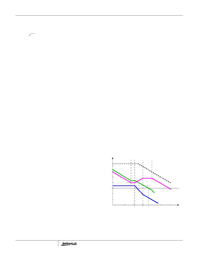
�Figure� 9� shows� an� asymptotic� plot� of� the� DC/DC� converter’s�
�gain� vs.� frequency.� The� actual� Modulator� Gain� has� a� high� gain�
�2.� Calculate� C1� such� that� F� Z1� is� placed� at� a� fraction� of� the� F� LC� ,�
�at� 0.1� to� 0.75� of� F� LC� (to� adjust,� change� the� 0.5� factor� to�
�desired� number).� The� higher� the� quality� factor� of� the� output�
�filter� and/or� the� higher� the� ratio� F� CE� /F� LC� ,� the� lower� the� F� Z1�
�frequency� (to� maximize� phase� boost).�
�peak� dependent� on� the� quality� factor� (Q)� of� the� output� filter,�
�which� is� not� shown.� Using� the� above� guidelines� should� yield� a�
�compensation� gain� similar� to� the� curve� plotted.� The� open� loop�
�error� amplifier� gain� bounds� the� compensation� gain.� Check� the�
�compensation� gain� at� F� P2� against� the� capabilities� of� the� error�
�amplifier.� The� closed� loop� gain,� G� CL� ,� is� constructed� on� the�
�C1� =� ------------------------------------------------�
�1�
�2� π� ?� R2� ?� 0.5� ?� F� LC�
�3.� Calculate� C2� such� that� F� P1� is� placed� at� F� CE� .�
�(EQ.� 10)�
�log-log� graph� of� Figure� 9� by� adding� the� modulator� gain,� G� MOD�
�(in� dB),� to� the� feedback� compensation� gain,� G� FB� (in� dB).� This�
�is� equivalent� to� multiplying� the� modulator� transfer� function� and�
�the� compensation� transfer� function� and� then� plotting� the�
�resulting� gain.�
�C2� =� ---------------------------------------------------------�
�C1�
�2� π� ?� R2� ?� C1� ?� F� CE� –� 1�
�(EQ.� 11)�
�F� Z1� F� Z2�
�F� P1�
�F� P2�
�MODULATOR� GAIN�
�COMPENSATION� GAIN�
�R3� =� ----------------------�
�F� SW�
�C3� =� -------------------------------------------------�
�20� log� ?� ?� ?� ?�
�d� MAX� ?� V�
�--------�
�IN�
�FREQUENCY�
�F� CE�
�F� LC�
�F� 0�
�4.� Calculate� R3� such� that� F� Z2� is� placed� at� F� LC� .� Calculate� C3�
�such� that� F� P2� is� placed� below� F� SW� (typically,� 0.5� to� 1.0�
�times� F� SW� ).� F� SW� represents� the� per-channel� switching�
�frequency.� Change� the� numerical� factor� to� reflect� desired�
�placement� of� this� pole.� Placement� of� F� P2� lower� in�
�frequency� helps� reduce� the� gain� of� the� compensation�
�network� at� high� frequency,� in� turn� reducing� the� HF� ripple�
�component� at� the� COMP� pin� and� minimizing� resultant�
�duty� cycle� jitter.�
�R1�
�------------� –� 1�
�F� LC� (EQ.� 12)�
�1�
�2� π� ?� R3� ?� 0.7� ?� F� SW�
�It� is� recommended� a� mathematical� model� is� used� to� plot� the�
�loop� response.� Check� the� loop� gain� against� the� error�
�amplifier� ’s� open-loop� gain.� Verify� phase� margin� results� and�
�adjust� as� necessary.� The� following� equations� describe� the�
�14�
�CLOSED� LOOP� GAIN�
�OPEN� LOOP� E/A� GAIN�
�R2�
�R1�
�20� log� ---------------------------------�
�0� V� OSC�
�G� FB�
�G� CL�
�G� MOD�
�LOG�
�FIGURE� 9.� ASYMPTOTIC� BODE� PLOT� OF� CONVERTER� GAIN�
�A� stable� control� loop� has� a� gain� crossing� with� close� to� a�
�-20dB/decade� slope� and� a� phase� margin� greater� than� 45°.�
�Include� worst� case� component� variations� when� determining�
�phase� margin.� The� mathematical� model� presented� makes� a�
�FN9222.1�
�July� 18,� 2007�
�相关PDF资料 |
PDF描述 |
|---|---|
| ISL6316IRZ | IC REG CTRLR BUCK PWM VM 40-QFN |
| ISL6322GIRZ-T | IC CTRLR PWM BUCK 48-QFN |
| ISL6322IRZ | IC CTRLR PWM 4PHASE BUCK 48-QFN |
| ISL6323AIRZ | IC PWM CTRLR SYNC BUCK DL 48QFN |
| ISL6323BIRZ | IC PWM CTRLR SYNC BUCK DL 48QFN |
相关代理商/技术参数 |
参数描述 |
|---|---|
| ISL6315IRZ-T | 功能描述:IC REG CTRLR BUCK PWM VM 24-QFN RoHS:是 类别:集成电路 (IC) >> PMIC - 稳压器 - DC DC 切换控制器 系列:- 产品培训模块:Lead (SnPb) Finish for COTS Obsolescence Mitigation Program 标准包装:2,500 系列:- PWM 型:电流模式 输出数:1 频率 - 最大:275kHz 占空比:50% 电源电压:18 V ~ 110 V 降压:无 升压:无 回扫:无 反相:无 倍增器:无 除法器:无 Cuk:无 隔离:是 工作温度:-40°C ~ 85°C 封装/外壳:8-SOIC(0.154",3.90mm 宽) 包装:带卷 (TR) |
| ISL6316CRZ | 功能描述:软开关 PWM 控制器 W/ANNEAL 4-PHS VR11 CNTRLR COM RoHS:否 制造商:Fairchild Semiconductor 输出端数量: 输出电流: 开关频率: 工作电源电压:30 V 电源电流: 最大工作温度:+ 105 C 最小工作温度:- 40 C 安装风格:SMD/SMT 封装 / 箱体:SOIC-8 封装:Reel |
| ISL6316CRZ-T | 功能描述:软开关 PWM 控制器 W/ANNEAL ISL6306 4-PHS VR11 CNTRLRCOM RoHS:否 制造商:Fairchild Semiconductor 输出端数量: 输出电流: 开关频率: 工作电源电压:30 V 电源电流: 最大工作温度:+ 105 C 最小工作温度:- 40 C 安装风格:SMD/SMT 封装 / 箱体:SOIC-8 封装:Reel |
| ISL6316IRZ | 功能描述:软开关 PWM 控制器 W/ANNEAL 4-PHS VR11 CNTRLR INDUSTRIAL RoHS:否 制造商:Fairchild Semiconductor 输出端数量: 输出电流: 开关频率: 工作电源电压:30 V 电源电流: 最大工作温度:+ 105 C 最小工作温度:- 40 C 安装风格:SMD/SMT 封装 / 箱体:SOIC-8 封装:Reel |
| ISL6316IRZ-T | 功能描述:软开关 PWM 控制器 W/ANNEAL ISL6306 CNTRLR INDUSTRIAL RoHS:否 制造商:Fairchild Semiconductor 输出端数量: 输出电流: 开关频率: 工作电源电压:30 V 电源电流: 最大工作温度:+ 105 C 最小工作温度:- 40 C 安装风格:SMD/SMT 封装 / 箱体:SOIC-8 封装:Reel |
发布紧急采购,3分钟左右您将得到回复。