- 您现在的位置:买卖IC网 > PDF目录17644 > ISL6328IRZ-T (Intersil)IC CTRLR PWM SYNC BUCK DL 48QFN PDF资料下载
参数资料
| 型号: | ISL6328IRZ-T |
| 厂商: | Intersil |
| 文件页数: | 27/33页 |
| 文件大小: | 0K |
| 描述: | IC CTRLR PWM SYNC BUCK DL 48QFN |
| 标准包装: | 4,000 |
| 应用: | 控制器,AMD SVI |
| 输入电压: | 5 V ~ 12 V |
| 输出数: | 2 |
| 输出电压: | 0.0125 V ~ 1.55 V |
| 工作温度: | -40°C ~ 85°C |
| 安装类型: | * |
| 封装/外壳: | * |
| 供应商设备封装: | * |
| 包装: | * |
第1页第2页第3页第4页第5页第6页第7页第8页第9页第10页第11页第12页第13页第14页第15页第16页第17页第18页第19页第20页第21页第22页第23页第24页第25页第26页当前第27页第28页第29页第30页第31页第32页第33页
�� �
�
�ISL6328�
�-------------------------------� >� f� 0�
�C� 2�
�1�
�2� ?� π� ?� L� ?� C�
�2� ?� π� ?� f� 0� ?� V� pp� ?� L� ?� C�
�2� ?� π� ?� V� PP� ?� R� FB� ?� f� 0�
�C� 1�
�R� C�
�C� C�
�COMP�
�FB�
�ISL6328�
�Case� 1:�
�0.66� ?� V�
�R� C� =� R� FB� ?� ------------------------------------------------------�
�IN�
�0.66� ?� V� IN�
�C� C� =� --------------------------------------------------�
�R� 1�
�R� FB�
�-------------------------------� ≤� f� 0� <� -----------------------------------�
�2� ?� π� ?� L� ?� C�
�VSEN�
�1� 1�
�2� ?� π� ?� C� ?� ESR�
�V� PP� ?� (� 2� ?� π� )� 2� ?� f� 02� ?� L� ?� C�
�C� C� =� ----------------------------------------------------------------------------------�
�PP� ?� R� FB� ?�
�(� 2� ?� π� )� 2� ?� f� 2� ?� V� L� ?� C�
�R� 1� =� R� FB� ?� ----------------------------------------�
�f� 0� >� -----------------------------------�
�2� ?� π� ?� f� 0� ?� V� pp� ?� L�
�0.66� ?� V� IN� ?� ESR�
�2� ?� π� ?� V� PP� ?� R� FB� ?� f� 0� ?� L�
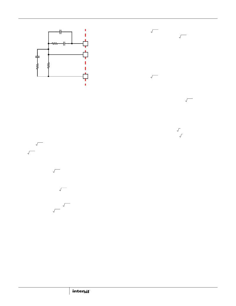
�FIGURE� 21.� COMPENSATION� CIRCUIT� WITHOUT� LOAD-LINE�
�REGULATION�
�The� first� step� is� to� choose� the� desired� bandwidth,� f� 0� ,� of� the�
�compensated� system.� Choose� a� frequency� high� enough� to� assure�
�adequate� transient� performance� but� not� higher� than� 1/3� of� the�
�switching� frequency.� The� type-III� compensator� has� an� extra�
�high-frequency� pole,� f� HF� .� This� pole� can� be� used� for� added� noise�
�rejection� or� to� assure� adequate� attenuation� at� the� error-amplifier�
�high� order� pole� and� zero� frequencies.� A� good� general� rule� is� to�
�choose� f� HF� =� 10f� 0� ,� but� it� can� be� higher� if� desired.� Choosing� f� HF� to�
�be� lower� than� 10f� 0� can� cause� problems� with� too� much� phase� shift�
�below� the� system� bandwidth.�
�C� ?� ESR�
�L� ?� C� –� C� ?� ESR�
�Case� 2:�
�Case� 3:�
�0.66� ?� V�
�R� C� =� R� FB� ?� ---------------------------------------------------------------�
�IN�
�0.66� ?� V� IN�
�0�
�1�
�2� ?� π� ?� C� ?� ESR�
�R� C� =� R� FB� ?� -------------------------------------------�
�0.66� ?� V� IN� ?� ESR� ?� C�
�C� C� =� --------------------------------------------------------------�
�(EQ.� 38)�
�C� 1� =� ----------------------------------------�
�L� ?� C� –� C� ?� ESR�
�R� FB�
�Output� Filter� Design�
�The� output� inductors� and� the� output� capacitor� bank� together� to�
�form� a� low-pass� filter� responsible� for� smoothing� the� pulsating�
�C� 2� =� -----------------------------------------------------------------------------------------------------�
�HF� ?� (� L� ?� C� )� ?� R� FB� ?� V� P� –� P�
�(� 2� ?� π� )� 2� ?� f� ?� f�
�V� PP� ?� ?� 2� π� ?� ?� f� 0� ?� f� HF� ?� L� ?� C� ?� R� FB�
�R� C� =� --------------------------------------------------------------------------------------�
�0.75� ?� V� ?� (� 2� ?� π� ?� f� HF� ?� L� ?� C� –� 1� )�
�0�
�?� ?�
�IN�
�2�
�0.75� ?� V� IN�
�(EQ.� 37)�
�voltage� at� the� phase� nodes.� The� output� filter� also� must� provide�
�the� transient� energy� until� the� regulator� can� respond.� Because� it�
�has� a� low� bandwidth� compared� to� the� switching� frequency,� the�
�output� filter� limits� the� system� transient� response.� The� output�
�capacitors� must� supply� or� sink� load� current� while� the� current� in�
�the� output� inductors� increases� or� decreases� to� meet� the�
�demand.�
�In� high-speed� converters,� the� output� capacitor� bank� is� usually� the�
�(� 2� ?� π� )� 2� ?� f� 0� ?� f� HF� ?� (� L� ?� C� )� ?� R� FB� ?� V� P� –� P�
�0.75� ?� V� IN� ?� (� 2� ?� π� ?� f� HF� ?� L� ?� C� –� 1� )�
�C� C� =� -----------------------------------------------------------------------------------------------------�
�In� the� solutions� to� the� compensation� equations,� there� is� a� single�
�degree� of� freedom.� For� the� solutions� presented� in� Equation� 38,�
�R� FB� is� selected� arbitrarily.� The� remaining� compensation�
�components� are� then� selected� according� to� Equation� 38.�
�In� Equation� 38,� L� is� the� per-channel� filter� inductance� divided� by�
�the� number� of� active� channels;� C� is� the� sum� total� of� all� output�
�capacitors;� ESR� is� the� equivalent-series� resistance� of� the� bulk�
�output-filter� capacitance;� and� V� PP� is� the� peak-to-peak� sawtooth�
�signal� amplitude� as� described� in� “Electrical� Specifications”� on�
��27�
�most� costly� (and� often� the� largest)� part� of� the� circuit.� Output� filter�
�design� begins� with� minimizing� the� cost� of� this� part� of� the� circuit.�
�The� critical� load� parameters� in� choosing� the� output� capacitors� are�
�the� maximum� size� of� the� load� step,� Δ� I,� the� load-current� slew� rate,�
�di/dt,� and� the� maximum� allowable� output-voltage� deviation� under�
�transient� loading,� Δ� V� MAX� .� Capacitors� are� characterized� according�
�to� their� capacitance,� ESR,� and� ESL� (equivalent� series� inductance).�
�FN7621.1�
�June� 7,� 2011�
�相关PDF资料 |
PDF描述 |
|---|---|
| LB16WGW01 | SWITCH PUSHBUTTON SPDT 3A 125V |
| ISL6328CRZ-T | IC CTRLR PWM SYNC BUCK DL 48QFN |
| LB16WKW01 | SWITCH PUSHBUTTON SPDT 3A 125V |
| X9315WMIZ-2.7T1R5419 | IC DGTL POT 32POS 10K 8MSOP |
| YB15WCKG01-BB | SWITCH PUSH SPDT 0.4VA 28V |
相关代理商/技术参数 |
参数描述 |
|---|---|
| ISL6329CRZ | 功能描述:电压模式 PWM 控制器 6+1 PHS DL PWM CONTRLR FOR CORE RoHS:否 制造商:Texas Instruments 输出端数量:1 拓扑结构:Buck 输出电压:34 V 输出电流: 开关频率: 工作电源电压:4.5 V to 5.5 V 电源电流:600 uA 最大工作温度:+ 125 C 最小工作温度:- 40 C 封装 / 箱体:WSON-8 封装:Reel |
| ISL6329CRZ-T | 功能描述:电压模式 PWM 控制器 6+1 PHS DL PWM CONTRLR FOR CORE RoHS:否 制造商:Texas Instruments 输出端数量:1 拓扑结构:Buck 输出电压:34 V 输出电流: 开关频率: 工作电源电压:4.5 V to 5.5 V 电源电流:600 uA 最大工作温度:+ 125 C 最小工作温度:- 40 C 封装 / 箱体:WSON-8 封装:Reel |
| ISL6329EVAL1Z | 制造商:Intersil Corporation 功能描述:ISL6329 EVALUATION BOARD - 60 LEAD - QFN - ROHS COMPLIANT - Bulk |
| ISL6329IRZ | 功能描述:电压模式 PWM 控制器 6+1 PHS DL PWM CONTRLR FOR CORE RoHS:否 制造商:Texas Instruments 输出端数量:1 拓扑结构:Buck 输出电压:34 V 输出电流: 开关频率: 工作电源电压:4.5 V to 5.5 V 电源电流:600 uA 最大工作温度:+ 125 C 最小工作温度:- 40 C 封装 / 箱体:WSON-8 封装:Reel |
| ISL6329IRZ-T | 功能描述:电压模式 PWM 控制器 6+1 PHS DL PWM CONTRLR FOR CORE RoHS:否 制造商:Texas Instruments 输出端数量:1 拓扑结构:Buck 输出电压:34 V 输出电流: 开关频率: 工作电源电压:4.5 V to 5.5 V 电源电流:600 uA 最大工作温度:+ 125 C 最小工作温度:- 40 C 封装 / 箱体:WSON-8 封装:Reel |
发布紧急采购,3分钟左右您将得到回复。