参数资料
| 型号: | ISL6353CRTZ-T |
| 厂商: | Intersil |
| 文件页数: | 12/30页 |
| 文件大小: | 0K |
| 描述: | IC CONTROLLER DDR VR12 40TQFN |
| 标准包装: | 6,000 |
| 应用: | 控制器,DDR,Intel VR12 |
| 输入电压: | 4.5 V ~ 25 V |
| 输出数: | 1 |
| 输出电压: | 0.25 V ~ 1.52 V |
| 工作温度: | 0°C ~ 70°C |
| 安装类型: | 表面贴装 |
| 封装/外壳: | 40-WFQFN 裸露焊盘 |
| 供应商设备封装: | 40-TQFN-EP(5x5) |
| 包装: | 带卷 (TR) |
第1页第2页第3页第4页第5页第6页第7页第8页第9页第10页第11页当前第12页第13页第14页第15页第16页第17页第18页第19页第20页第21页第22页第23页第24页第25页第26页第27页第28页第29页第30页
�� �
�
�ISL6353�
�VW�
�voltage� V� Crs� hits� VW,� the� slave� circuit� turns� off� the� PWM� pulse,�
�and� the� current� source� discharges� C� rs� .�
�Since� the� ISL6353� individual� phase� modulators� use� a�
�Vcrm�
�Master�
�Clock�
�Clock1�
�PWM1�
�Clock2�
�PWM2�
�Clock3�
�PWM3�
�COMP�
�VW�
�large-amplitude� and� noise-free� synthesized� signal,� V� crs� ,� to�
�determine� the� pulse� width,� phase� jitter� is� lower� than� conventional�
�hysteretic� mode� and� fixed� PWM� mode� controllers.� Unlike�
�conventional� hysteretic� mode� converters,� the� ISL6353� has� an�
�error� amplifier� that� allows� the� controller� to� maintain� 0.5%� output�
�voltage� accuracy.�
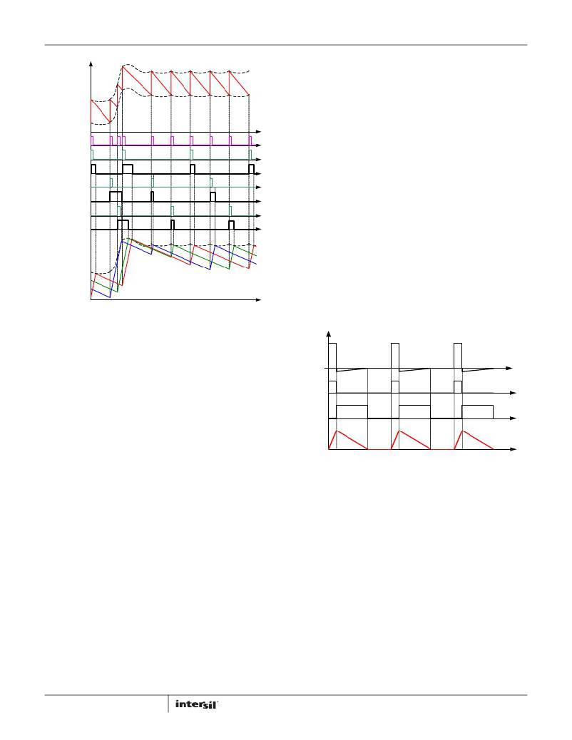
�Figure� 5� shows� the� principle� of� operation� during� a� load� step-up�
�response.� The� COMP� voltage� rises� after� the� load� step� up,�
�generating� master� clock� pulses� more� quickly,� so� PWM� pulses�
�turn� on� earlier,� increasing� the� effective� switching� frequency.� This�
�allows� for� higher� control� loop� bandwidth� than� conventional� fixed�
�frequency� PWM� controllers.� The� VW� voltage� rises� as� the� COMP�
�voltage� rises,� making� the� PWM� pulses� wider� as� well.� During� load�
�step-down� response,� COMP� voltage� falls.� It� takes� the� master�
�clock� circuit� longer� to� generate� the� next� clock� signal,� so� the� PWM�
�pulse� is� held� off� until� needed.� The� VW� voltage� falls� as� the� COMP�
�voltage� falls,� reducing� the� current� PWM� pulse� width.� This� kind� of�
�behavior� gives� the� ISL6353� excellent� load� transient� response.�
�Vcrs1�
�Vcrs3�
�Vcrs2�
�FIGURE� 5.� R� 3� MODULATOR� OPERATION� DURING� A� LOAD�
�STEP-UP� RESPONSE�
�The� ISL6353� is� a� multiphase� regulator� controller� implementing�
�the� Intel� VR12?� protocol� primarily� intended� for� use� in� DDR�
�memory� regulator� applications.� It� can� be� programmed� for� 1-,� 2-� or�
�3-phase� operation.� It� uses� Intersil’s� patented� R� 3� (Robust� Ripple�
�Regulator?)� modulator.� The� R� 3� modulator� combines� the� best�
�features� of� fixed� frequency� PWM� and� hysteretic� PWM� while�
�eliminating� many� of� their� respective� shortcomings.� Figure� 3�
�conceptually� shows� the� ISL6353� multiphase� R� 3� modulator� circuit,�
�and� Figure� 4� shows� the� principle� of� operation.�
�A� current� source� flows� from� the� VW� pin� to� the� COMP� pin,� creating�
�a� voltage� window� set� by� the� resistor� between� the� two� pins.� This�
�voltage� window� is� called� the� VW� window� in� the� following�
�discussion.�
�Inside� the� IC,� the� modulator� uses� the� master� clock� circuit� to�
�generate� the� clocks� for� the� slave� circuits.� The� modulator� discharges�
�the� ripple� capacitor� C� rm� with� a� current� source� equal� to� g� m� V� o� ,� where�
�g� m� is� a� gain� factor.� The� C� rm� voltage� V� crm� is� a� sawtooth� waveform�
�traversing� between� the� VW� and� COMP� voltages.� It� resets� to� VW�
�when� it� hits� COMP,� and� generates� a� one-shot� master� clock� signal.� A�
�phase� sequencer� distributes� the� master� clock� signal� to� the� slave�
�circuits.� If� the� ISL6353� is� in� 3-phase� mode,� the� master� clock� signal�
�will� be� distributed� to� the� three� phases,� and� the� Clock1~3� signals� will�
�be� 120°� out-of-phase.� If� the� ISL6353� is� in� 2-phase� mode,� the�
�master� clock� signal� will� be� distributed� to� Phases� 1� and� 2,� and� the�
�Clock1� and� Clock2� signals� will� be� 180°� out-of-phase.� If� the� ISL6353�
�is� in� 1-phase� mode,� the� master� clock� signal� will� be� distributed� to�
�Phase� 1� only� and� is� the� Clock1� signal.�
�Each� slave� circuit� has� its� own� ripple� capacitor� C� rs� ,� whose� voltage�
�mimics� the� inductor� ripple� current.� A� g� m� amplifier� converts� the�
�inductor� voltage� into� a� current� source� to� charge� and� discharge�
�C� rs� .� The� slave� circuit� turns� on� its� PWM� pulse� upon� receiving� the�
�clock� signal,� and� the� current� source� charges� C� rs� .� When� C� rs�
�12�
�The� fact� that� all� the� phases� share� the� same� VW� window� voltage�
�also� ensures� excellent� dynamic� current� balance� among� phases.�
�Diode� Emulation� and� Period� Stretching�
�PHASE�
�UG� ATE�
�LG� ATE�
�IL�
�FIGURE� 6.� DIODE� EMULATION� OPERATION�
�ISL6353� can� operate� in� diode� emulation� (DE)� mode� to� improve�
�light� load� efficiency.� In� DE� mode,� the� low-side� MOSFET� conducts�
�when� the� current� is� flowing� from� source� to� drain� and� does� not�
�allow� reverse� current,� thus� emulating� a� diode.� As� Figure� 6� shows,�
�when� LGATE� is� on,� the� low-side� MOSFET� carries� current,� creating�
�negative� voltage� on� the� phase� node� due� to� the� voltage� drop� across�
�the� ON-resistance.� The� ISL6353� monitors� the� current� by�
�monitoring� the� phase� node� voltage.� It� turns� off� LGATE� when� the�
�phase� node� voltage� reaches� zero� to� prevent� the� inductor� current�
�from� reversing� direction� and� creating� unnecessary� power� loss.�
�If� the� load� current� is� light� enough,� as� Figure� 6� shows,� the� inductor�
�current� will� reach� and� stay� at� zero� before� the� next� phase� node�
�pulse,� and� the� regulator� is� in� discontinuous� conduction� mode�
�(DCM).� If� the� load� current� is� heavy� enough,� the� inductor� current�
�will� never� reach� 0A,� and� the� regulator� is� in� CCM� although� the�
�controller� is� in� DE� mode.�
�September� 15,� 2011�
�FN6897.0�
�相关PDF资料 |
PDF描述 |
|---|---|
| ISL6566ACRZ | IC CTRLR PWM 3PHASE BUCK 40-QFN |
| ACM25DSES-S243 | CONN EDGECARD 50POS .156 EYELET |
| 2510-28K | INDUCTOR RF 1.5UH UNSHIELDED SMD |
| LT1175IS8-5#PBF | IC REG LDO -5V .5A 8SOIC |
| LT1175IS8#PBF | IC REG LDO NEG ADJ .5A 8SOIC |
相关代理商/技术参数 |
参数描述 |
|---|---|
| ISL6353CRTZ-TS2568 | 制造商:Intersil Corporation 功能描述:INTEL, ISL6353CRTZ-T W/BARCODE LABELS, 12 MONTH D/C RESTRICT - Tape and Reel |
| ISL6353CRZ | 制造商:Intersil 功能描述:Multiphase PWM Regulator for VR12 DDR Memory Systems |
| ISL6353IRTZ | 功能描述:电流型 PWM 控制器 VR12 MEMORY CNTRLR 3 PHS 2 INT 5V DRVRS RoHS:否 制造商:Texas Instruments 开关频率:27 KHz 上升时间: 下降时间: 工作电源电压:6 V to 15 V 工作电源电流:1.5 mA 输出端数量:1 最大工作温度:+ 105 C 安装风格:SMD/SMT 封装 / 箱体:TSSOP-14 |
| ISL6353IRTZ-T | 功能描述:电流型 PWM 控制器 VR12 MEMORY CNTRLR 3 PHS 2 INT 5V DRVRS RoHS:否 制造商:Texas Instruments 开关频率:27 KHz 上升时间: 下降时间: 工作电源电压:6 V to 15 V 工作电源电流:1.5 mA 输出端数量:1 最大工作温度:+ 105 C 安装风格:SMD/SMT 封装 / 箱体:TSSOP-14 |
| ISL6363CRTZ | 功能描述:IC CONTROLLER VR12 48TQFN RoHS:是 类别:集成电路 (IC) >> PMIC - 稳压器 - 专用型 系列:- 标准包装:43 系列:- 应用:控制器,Intel VR11 输入电压:5 V ~ 12 V 输出数:1 输出电压:0.5 V ~ 1.6 V 工作温度:-40°C ~ 85°C 安装类型:表面贴装 封装/外壳:48-VFQFN 裸露焊盘 供应商设备封装:48-QFN(7x7) 包装:管件 |
发布紧急采购,3分钟左右您将得到回复。