- 您现在的位置:买卖IC网 > PDF目录15064 > ISL6526AIB-T (Intersil)IC REG CTRLR BUCK PWM VM 14-SOIC PDF资料下载
参数资料
| 型号: | ISL6526AIB-T |
| 厂商: | Intersil |
| 文件页数: | 10/15页 |
| 文件大小: | 0K |
| 描述: | IC REG CTRLR BUCK PWM VM 14-SOIC |
| 标准包装: | 2,500 |
| PWM 型: | 电压模式 |
| 输出数: | 1 |
| 频率 - 最大: | 650kHz |
| 占空比: | 100% |
| 电源电压: | 2.97 V ~ 3.63 V |
| 降压: | 是 |
| 升压: | 无 |
| 回扫: | 无 |
| 反相: | 无 |
| 倍增器: | 无 |
| 除法器: | 无 |
| Cuk: | 无 |
| 隔离: | 无 |
| 工作温度: | 0°C ~ 70°C |
| 封装/外壳: | 14-SOIC(0.154",3.90mm 宽) |
| 包装: | 带卷 (TR) |
�� �
�
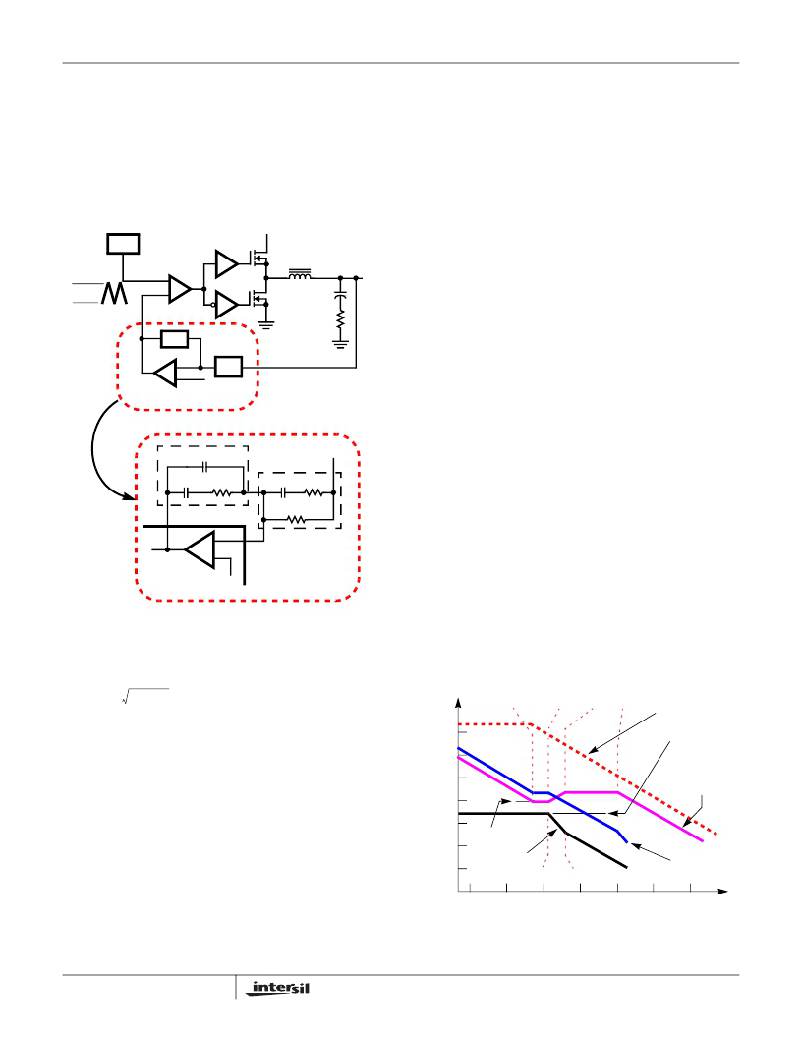
�ISL6526,� ISL6526A�
�the� PHASE� node.� The� PWM� wave� is� smoothed� by� the� output�
�filter� (L� O� and� C� O� ).�
�The� modulator� transfer� function� is� the� small-signal� transfer�
�function� of� V� OUT� /V� E/A� .� This� function� is� dominated� by� a� DC�
�Gain� and� the� output� filter� (L� O� and� C� O� ),� with� a� double� pole�
�break� frequency� at� f� LC� and� a� zero� at� f� ESR� .� The� DC� Gain� of�
�the� modulator� is� simply� the� input� voltage� (V� IN� )� divided� by� the�
�peak-to-peak� oscillator� voltage� Δ� V� OSC� .�
�2.� Place� first� zero� below� filter’s� double� pole� (~75%� f� LC� ).�
�3.� Place� second� zero� at� filter� ’s� double� pole.�
�4.� Place� first� pole� at� the� ESR� zero.�
�5.� Place� second� pole� at� half� the� switching� frequency.�
�6.� Check� gain� against� error� amplifier� ’s� open-loop� gain.�
�7.� Estimate� phase� margin� -� repeat� if� necessary.�
�Compensation� Break� Frequency� Equations�
�f� Z1� =� ----------------------------------�
�OSC�
�DRIVER�
�V� IN�
�1�
�2� π� ×� R� 2� ×� C� 2�
�(EQ.� 6)�
�f� Z2� =� -------------------------------------------------------�
�f� P1� =� ---------------------------------------------------------�
�2� π� x� R� 2� x� ?� ?�
�?� C� 1� x� C� 2� ?�
�f� P2� =� ------------------------------------�
�Δ� V� OSC�
�PWM�
�COMPARATOR�
�-�
�+�
�Z� FB�
�V� E/A�
�-�
�+�
�DRIVER�
�Z� IN�
�L� O�
�PHASE�
�C� O�
�ESR�
�(PARASITIC)�
�V� OUT�
�1�
�2� π� x� (� R� 1� +� R� 3� )� x� C� 3�
�1�
�----------------------�
�?� C� 1� +� C� 2� ?�
�1�
�2� π� x� R� 3� x� C� 3�
�(EQ.� 7)�
�(EQ.� 8)�
�(EQ.� 9)�
�ERROR�
�AMP�
�REFERENCE�
�Figure� 6� shows� an� asymptotic� plot� of� the� DC/DC� converter’s�
�DETAILED� COMPENSATION� COMPONENTS�
�gain� vs� frequency.� The� actual� Modulator� Gain� has� a� high� gain�
�peak� due� to� the� high� Q� factor� of� the� output� filter� and� is� not�
�C� 2�
�C� 1�
�R� 2�
�Z� FB�
�C� 3�
�Z� IN�
�R� 3�
�V� OUT�
�shown� in� Figure� 6.� Using� the� previously� mentioned� guidelines�
�should� give� a� Compensation� Gain� similar� to� the� curve� plotted.�
�The� open� loop� error� amplifier� gain� bounds� the� compensation�
�gain.� Check� the� compensation� gain� at� f� P2� with� the� capabilities�
�COMP�
�-�
�FB�
�R� 1�
�of� the� error� amplifier.� The� Closed� Loop� Gain� is� constructed� on�
�the� graph� of� Figure� 6� by� adding� the� Modulator� Gain� (in� dB)� to�
�the� Compensation� Gain� (in� dB).� This� is� equivalent� to�
�+�
�ISL6526,� ISL6526A�
�REFERENCE�
�FIGURE� 5.� VOLTAGE-MODE� BUCK� CONVERTER�
�COMPENSATION� DESIGN�
�Modulator� Break� Frequency� Equations�
�multiplying� the� modulator� transfer� function� to� the�
�compensation� transfer� function� and� plotting� the� gain.�
�The� compensation� gain� uses� external� impedance� networks�
�Z� FB� and� Z� IN� to� provide� a� stable,� high� bandwidth� (BW)� overall�
�loop.� A� stable� control� loop� has� a� gain� crossing� with�
�-20dB/decade� slope� and� a� phase� margin� greater� than�
�45°.� Include� worst� case� component� variations� when�
�f� LC� =� ------------------------------------------�
�f� ESR� =� -------------------------------------------�
�?� V� IN� ?�
�1�
�2� π� x� L� O� x� C� O�
�1�
�2� π� x� ESR� x� C� O�
�(EQ.� 4)�
�(EQ.� 5)�
�determining� phase� margin.�
�f� Z1� f� Z2�
�100�
�80�
�60�
�f� P1�
�f� P2�
�OPEN� LOOP�
�ERROR� AMP� GAIN�
�20� log� ?� ------------------� ?�
�?� V� OSC� ?�
�The� compensation� network� consists� of� the� error� amplifier�
�20� log� ?� --------� ?�
�(internal� to� the� ISL6526,� ISL6526A)� and� the� impedance�
�networks� Z� IN� and� Z� FB� .� The� goal� of� the� compensation�
�network� is� to� provide� a� closed� loop� transfer� function� with� the�
�highest� 0dB� crossing� frequency� (f� 0dB� )� and� adequate� phase�
�margin.� Phase� margin� is� the� difference� between� the� closed�
�40�
�20�
�0�
�-20�
�R2�
�?� R1� ?�
�COMPENSATION�
�GAIN�
�loop� phase� at� f� 0dB� and� 180°.� Equations� 6,� 7,� 8� and� 9� relate�
�the� compensation� network’s� poles,� zeros� and� gain� to� the�
�-40�
�MODULATOR�
�GAIN�
�f� LC�
�f� ESR�
�LOOP� GAIN�
�components� (R� 1� ,� R� 2� ,� R� 3� ,� C� 1� ,� C� 2� ,� and� C� 3� )� in� Figure� 5.� Use�
�these� guidelines� for� locating� the� poles� and� zeros� of� the�
�compensation� network:�
�1.� Pick� gain� (R� 2� /R� 1� )� for� desired� converter� bandwidth.�
�10�
�-60�
�10� 100� 1k� 10k� 100k� 1M� 10M�
�FREQUENCY� (Hz)�
�FIGURE� 6.� ASYMPTOTIC� BODE� PLOT� OF� CONVERTER� GAIN�
�FN9055.10�
�November� 24,� 2008�
�相关PDF资料 |
PDF描述 |
|---|---|
| X5045M8Z | IC CPU SUPERV 4K EE RST 8-MSOP |
| ISL6526AIB | IC REG CTRLR BUCK PWM VM 14-SOIC |
| X4043M8Z-2.7A | IC CPU SUPERV 4K EEPROM 8-MSOP |
| VI-2WW-EW-F3 | CONVERTER MOD DC/DC 5.5V 100W |
| X4043M8Z-4.5A | IC CPU SUPERV 4K EEPROM 8-MSOP |
相关代理商/技术参数 |
参数描述 |
|---|---|
| ISL6526AIR | 功能描述:电压模式 PWM 控制器 Single Synch Buck RoHS:否 制造商:Texas Instruments 输出端数量:1 拓扑结构:Buck 输出电压:34 V 输出电流: 开关频率: 工作电源电压:4.5 V to 5.5 V 电源电流:600 uA 最大工作温度:+ 125 C 最小工作温度:- 40 C 封装 / 箱体:WSON-8 封装:Reel |
| ISL6526AIR-T | 功能描述:IC REG CTRLR BUCK PWM VM 16-QFN RoHS:否 类别:集成电路 (IC) >> PMIC - 稳压器 - DC DC 切换控制器 系列:- 标准包装:4,000 系列:- PWM 型:电压模式 输出数:1 频率 - 最大:1.5MHz 占空比:66.7% 电源电压:4.75 V ~ 5.25 V 降压:是 升压:无 回扫:无 反相:无 倍增器:无 除法器:无 Cuk:无 隔离:无 工作温度:-40°C ~ 85°C 封装/外壳:40-VFQFN 裸露焊盘 包装:带卷 (TR) |
| ISL6526AIRZ | 功能描述:电压模式 PWM 控制器 600KHZ SNG PWM W/CHA RGE PUMP 16LD 5X5 RoHS:否 制造商:Texas Instruments 输出端数量:1 拓扑结构:Buck 输出电压:34 V 输出电流: 开关频率: 工作电源电压:4.5 V to 5.5 V 电源电流:600 uA 最大工作温度:+ 125 C 最小工作温度:- 40 C 封装 / 箱体:WSON-8 封装:Reel |
| ISL6526AIRZ-T | 功能描述:电压模式 PWM 控制器 600KHZ SINGLE PWM W/CHRG PUMP 16LD 5X5 RoHS:否 制造商:Texas Instruments 输出端数量:1 拓扑结构:Buck 输出电压:34 V 输出电流: 开关频率: 工作电源电压:4.5 V to 5.5 V 电源电流:600 uA 最大工作温度:+ 125 C 最小工作温度:- 40 C 封装 / 箱体:WSON-8 封装:Reel |
| ISL6526AIRZ-TK | 功能描述:IC REG CTRLR BUCK PWM VM 16-QFN RoHS:是 类别:集成电路 (IC) >> PMIC - 稳压器 - DC DC 切换控制器 系列:- 产品培训模块:Lead (SnPb) Finish for COTS Obsolescence Mitigation Program 标准包装:2,500 系列:- PWM 型:电流模式 输出数:1 频率 - 最大:275kHz 占空比:50% 电源电压:18 V ~ 110 V 降压:无 升压:无 回扫:无 反相:无 倍增器:无 除法器:无 Cuk:无 隔离:是 工作温度:-40°C ~ 85°C 封装/外壳:8-SOIC(0.154",3.90mm 宽) 包装:带卷 (TR) |
发布紧急采购,3分钟左右您将得到回复。