- 您现在的位置:买卖IC网 > PDF目录176104 > ISL6537A (Intersil Corporation) ACPI Regulator/Controller for Dual Channel DDR Memory Systems PDF资料下载
参数资料
| 型号: | ISL6537A |
| 厂商: | Intersil Corporation |
| 英文描述: | ACPI Regulator/Controller for Dual Channel DDR Memory Systems |
| 中文描述: | ACPI的稳压器/双通道DDR内存控制器系统 |
| 文件页数: | 4/15页 |
| 文件大小: | 488K |
| 代理商: | ISL6537A |
12
FN9143.3
Modulator Break Frequency Equations
The compensation network consists of the error amplifier
(internal to the ISL6537A) and the impedance networks ZIN
and ZFB. The goal of the compensation network is to provide
a closed loop transfer function with the highest 0dB crossing
frequency (f0dB) and adequate phase margin. Phase margin
is the difference between the closed loop phase at f0dB and
180 degrees. The equations below relate the compensation
network’s poles, zeros and gain to the components (R1, R2,
R3, C1, C2, and C3) in Figure 3. Use these guidelines for
locating the poles and zeros of the compensation network:
1. Pick Gain (R2/R1) for desired converter bandwidth.
2. Place 1ST Zero Below Filter’s Double Pole (~75% FLC).
3. Place 2ND Zero at Filter’s Double Pole.
4. Place 1ST Pole at the ESR Zero.
5. Place 2ND Pole at Half the Switching Frequency.
6. Check Gain against Error Amplifier’s Open-Loop Gain.
7. Estimate Phase Margin - Repeat if Necessary.
Compensation Break Frequency Equations
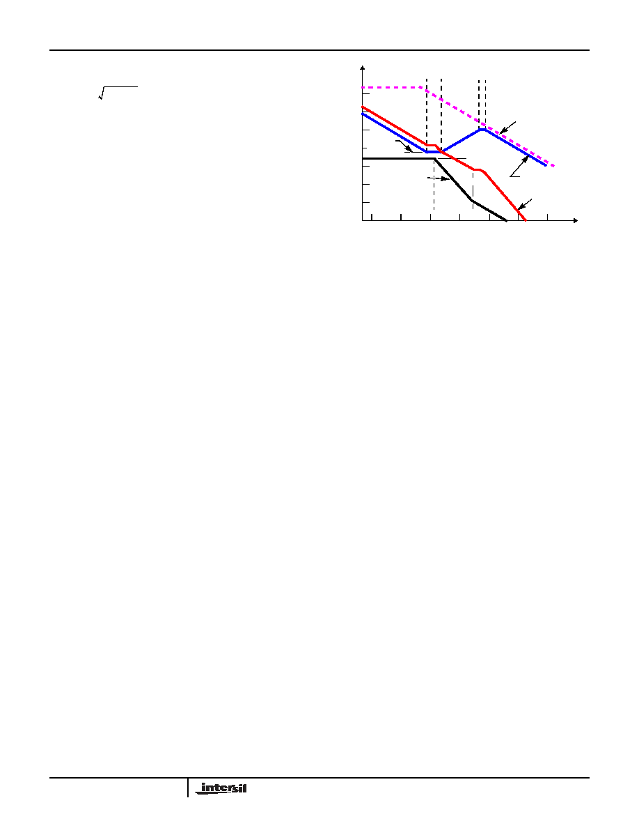
Figure 4 shows an asymptotic plot of the DC-DC converter’s
gain vs. frequency. The actual Modulator Gain has a high gain
peak due to the high Q factor of the output filter and is not
shown in Figure 6. Using the above guidelines should give a
Compensation Gain similar to the curve plotted. The open
loop error amplifier gain bounds the compensation gain.
Check the compensation gain at FP2 with the capabilities of
the error amplifier. The Closed Loop Gain is constructed on
the graph of Figure 4 by adding the Modulator Gain (in dB) to
the Compensation Gain (in dB). This is equivalent to
multiplying the modulator transfer function to the
compensation transfer function and plotting the gain.
The compensation gain uses external impedance networks
ZFB and ZIN to provide a stable, high bandwidth (BW) overall
loop. A stable control loop has a gain crossing with
-20dB/decade slope and a phase margin greater than 45
degrees. Include worst case component variations when
determining phase margin.
Output Voltage Selection
The output voltage of all the external voltage regulators can
be programmed to any level between their individual input
voltage and the internal reference, 0.8V. An external resistor
divider is used to scale the output voltage relative to the
reference voltage and feed it back to the inverting input of the
error amplifier, refer to the Typical Application on page 3.
The output voltage programming resistor will depend on the
value chosen for the feedback resistor and the desired
output voltage of the particular regulator.
If the output voltage desired is 0.8V, simply route the output
voltage back to the respective FB pin through the feedback
resistor and do not populate the output voltage programming
resistor.
The output voltage for the internal VTT_DDR linear regulator
is set internal to the ISL6537A to track the VDDQ voltage by
50%. There is no need for external programming resistors.
F
LC
1
2
π x L
O
x C
O
-------------------------------------------
=
F
ESR
1
2
π x ESR x C
O
--------------------------------------------
=
FZ1
1
2
π x R
2 x C1
------------------------------------
=
FZ2
1
2
π x R
1
R3
+
() x C
3
-------------------------------------------------------
=
FP1
1
2
π x R
2 x
C1 x C2
C1 C2
+
----------------------
---------------------------------------------------------
=
FP2
1
2
π x R
3 x C3
------------------------------------
=
100
80
60
40
20
0
-20
-40
-60
FP1
FZ2
10M
1M
100K
10K
1K
100
10
OPEN LOOP
ERROR AMP GAIN
FZ1
FP2
20LOG
FLC
FESR
COMPENSATION
GA
IN
(
d
B)
FREQUENCY (Hz)
GAIN
20LOG
(VIN/VOSC)
MODULATOR
GAIN
(R2/R1)
FIGURE 4. ASYMPTOTIC BODE PLOT OF CONVERTER GAIN
CLOSED LOOP
GAIN
R4
R1
0.8V
×
V
DDQ
0.8V
∠
-------------------------------------
=
R8
R5
0.8V
×
V
GMCH
0.8V
∠
-----------------------------------------
=
R10
R9
0.8V
×
V
xxxxxxxxxxxx
0.8V
∠
------------------------------------------------------------
=
R12
R11
0.8V
×
V
DAC
0.8V
∠
------------------------------------
=
TT_GMCH/CPU
ISL6537A
相关PDF资料 |
PDF描述 |
|---|---|
| ISL6612BIRZ-T | Advanced Synchronous Rectified Buck MOSFET Drivers with Pre-POR OVP |
| ISL6613BIRZ-T | Advanced Synchronous Rectified Buck MOSFET Drivers with Pre-POR OVP |
| ISL6740IBZ | Flexible Double Ended Voltage and Current Mode PWM Controllers |
| ISL6740IVZ | Flexible Double Ended Voltage and Current Mode PWM Controllers |
| ISL6741IBZ | Flexible Double Ended Voltage and Current Mode PWM Controllers |
相关代理商/技术参数 |
参数描述 |
|---|---|
| ISL6537A-6506EVAL1Z | 功能描述:EVALUATION BOARD ISL986A-6506 RoHS:是 类别:编程器,开发系统 >> 评估板 - DC/DC 与 AC/DC(离线)SMPS 系列:- 产品培训模块:Obsolescence Mitigation Program 标准包装:1 系列:True Shutdown™ 主要目的:DC/DC,步升 输出及类型:1,非隔离 功率 - 输出:- 输出电压:- 电流 - 输出:1A 输入电压:2.5 V ~ 5.5 V 稳压器拓扑结构:升压 频率 - 开关:3MHz 板类型:完全填充 已供物品:板 已用 IC / 零件:MAX8969 |
| ISL6537ACR | 功能描述:IC REG/CTRLR ACPI DUAL DDR 28QFN RoHS:否 类别:集成电路 (IC) >> PMIC - 电源管理 - 专用 系列:- 应用说明:Ultrasound Imaging Systems Application Note 产品培训模块:Lead (SnPb) Finish for COTS Obsolescence Mitigation Program 标准包装:37 系列:- 应用:医疗用超声波成像,声纳 电流 - 电源:- 电源电压:2.37 V ~ 6 V 工作温度:0°C ~ 70°C 安装类型:表面贴装 封装/外壳:56-WFQFN 裸露焊盘 供应商设备封装:56-TQFN-EP(8x8) 包装:管件 |
| ISL6537ACRR5160 | 制造商:Intersil Corporation 功能描述: |
| ISL6537ACR-T | 功能描述:IC REG/CTRLR ACPI DUAL DDR 28QFN RoHS:否 类别:集成电路 (IC) >> PMIC - 电源管理 - 专用 系列:- 应用说明:Ultrasound Imaging Systems Application Note 产品培训模块:Lead (SnPb) Finish for COTS Obsolescence Mitigation Program 标准包装:37 系列:- 应用:医疗用超声波成像,声纳 电流 - 电源:- 电源电压:2.37 V ~ 6 V 工作温度:0°C ~ 70°C 安装类型:表面贴装 封装/外壳:56-WFQFN 裸露焊盘 供应商设备封装:56-TQFN-EP(8x8) 包装:管件 |
| ISL6537ACRZ | 功能描述:IC REG/CTRLR ACPI DUAL DDR 28QFN RoHS:是 类别:集成电路 (IC) >> PMIC - 电源管理 - 专用 系列:- 应用说明:Ultrasound Imaging Systems Application Note 产品培训模块:Lead (SnPb) Finish for COTS Obsolescence Mitigation Program 标准包装:37 系列:- 应用:医疗用超声波成像,声纳 电流 - 电源:- 电源电压:2.37 V ~ 6 V 工作温度:0°C ~ 70°C 安装类型:表面贴装 封装/外壳:56-WFQFN 裸露焊盘 供应商设备封装:56-TQFN-EP(8x8) 包装:管件 |
发布紧急采购,3分钟左右您将得到回复。