参数资料
| 型号: | ISL6539CA |
| 厂商: | Intersil |
| 文件页数: | 14/20页 |
| 文件大小: | 0K |
| 描述: | IC CTRLR DDR DRAM, SDRAM 28QSOP |
| 标准包装: | 48 |
| 应用: | 控制器,DDR DRAM,SDRAM |
| 输入电压: | 3.3 V ~ 18 V |
| 输出数: | 2 |
| 输出电压: | 0.9 V ~ 5.5 V |
| 工作温度: | 0°C ~ 70°C |
| 安装类型: | 表面贴装 |
| 封装/外壳: | 28-SSOP(0.154",3.90mm 宽) |
| 供应商设备封装: | 28-SSOP/QSOP |
| 包装: | 管件 |
�� �
�
�ISL6539�
�channel� controller� are� disabled� when� the� DDR� pin� is� set�
�high.� As� the� VTT� channel� tracks� the� VDDQ/2� voltage,� the�
�soft-start� function� is� not� required,� and� the� SOFT2� pin� may� be�
�left� open,� in� the� event� both� channels� are� enabled�
�simultaneously.� However,� if� the� VTT� channel� is� enabled� later�
�than� the� VDDQ,� the� SOFT2� pin� must� have� a� capacitor� in�
�place� to� ensure� soft-start.� In� case� of� overcurrent� or�
�undervoltage� caused� by� short� circuit� on� VTT,� the� fault� current�
�will� propagate� to� the� first� channel� and� shut� down� the�
�converter.�
�1.� the� quiescent� current,� supporting� the� internal� logic� and�
�normal� operation� of� the� IC�
�2.� the� gate� driver� current� for� the� lower� MOSFETs�
�3.� and� the� current� going� through� the� external� diodes� to� the�
�bootstrap� capacitor� for� upper� MOSFET.�
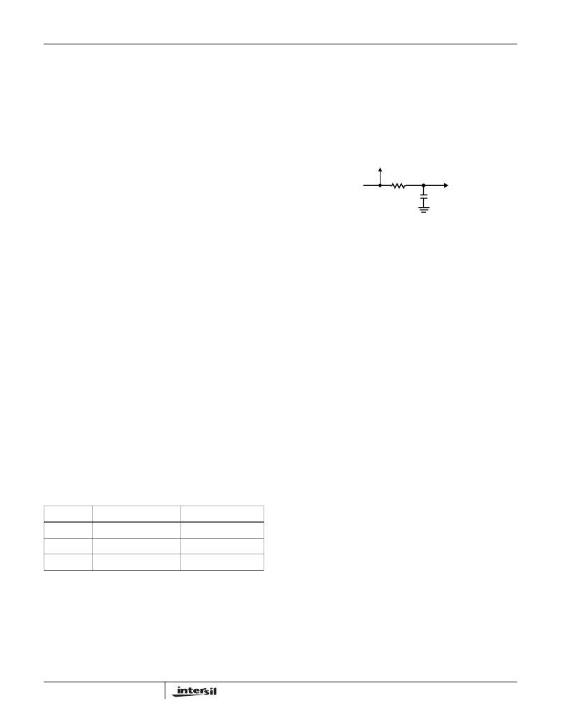
�In� order� to� reduce� the� noisy� effect� of� the� bootstrap� capacitor�
�current� to� the� IC,� a� small� resistor,� such� as� 10� Ω� ,� can� be� used�
�with� the� decoupling� cap� to� construct� a� low� pass� filter� for� the�
�IC,� as� shown� in� Figure� 11.�
�TO� BOOT�
�The� VREF� voltage� will� be� present� even� if� the� VTT� is�
�disabled.�
�5V�
�VCC�
�I� SOURCING� (� 140� Ω� +� R� CS� )� =� I� D� r� DS� (� ON� )�
�Channel� Synchronization� in� DDR� Applications�
�The� presence� of� two� PWM� controllers� on� the� same� die�
�requires� channel� synchronization,� to� reduce� inter-channel�
�interference� that� may� cause� the� duty� factor� jitter� and�
�increased� output� ripple.�
�The� PWM� controller� is� at� greatest� noise� susceptibility� when�
�an� error� signal� on� the� input� of� the� PWM� comparator�
�approaches� the� decision-making� point.� False� triggering� may�
�occur,� causing� jitter� and� affecting� the� output� regulation.�
�A� common� approach� used� to� synchronize� dual� channel�
�converters� is� out-of-phase� operation.� Out-of-phase�
�operation� reduces� input� current� ripple� and� provides� a�
�minimum� interference� for� channels� that� control� different�
�voltage� levels.�
�When� used� in� a� DDR� application� with� cascaded� converters�
�(VTT� generated� from� VDDQ),� several� methods� of�
�synchronization� are� implemented� in� the� ISL6539.� When� the�
�DDR� pin� is� connected� to� GND� for� dual� switcher� applications,�
�the� channels� operate� 180°� out-of-phase.� In� the� DDR� mode,�
�when� the� DDR� pin� is� connected� to� VCC,� the� channels�
�operate� either� with� 0°� phase� shift,� when� the� VIN� pin� is�
�connected� to� the� GND,� or� with� 90°� phase� shift� if� the� VIN� pin�
�is� connected� to� a� voltage� higher� than� 4.2V.�
�The� following� table� lists� the� different� synchronization�
�schemes� and� their� usage:�
�DDR� PIN� VIN� PIN� SYNCHRONIZATION�
�10� Ω�
�FIGURE� 11.� INPUT� FILTERING� FOR� THE� CHIP�
�The� soft-start� capacitor� and� the� resistor� divider� setting� the�
�output� voltage� is� easy� to� select� as� discussed� in� the� “Block�
��Selection� of� the� Current� Sense� Resistor�
�The� value� of� the� current� sense� resistor� determines� the� gain�
�of� the� current� sensing� circuit.� It� affects� the� current� loop� gain�
�and� the� overcurrent� protection� setpoint.� The� voltage� drop� on�
�the� lower� MOSFET� is� sensed� within� 400ns� after� the� upper�
�MOSFET� is� turned� off.� The� current� sense� pin� has� a� 140� Ω�
�resistor� in� series� with� the� external� current� sensing� resistor.�
�The� current� sense� pin� can� source� up� to� a� 260μA� current�
�while� sensing� current� on� the� lower� MOSFET,� in� such� a� way�
�that� the� voltage� drop� on� the� current� sensing� path� would�
�equal� to� the� voltage� on� the� MOSFET.�
�(EQ.� 16)�
�I� D� can� be� assumed� to� be� the� inductor� peak� current.� In� a�
�worst� case� scenario,� the� high� temperature� r� DS(ON)� could�
�increase� to� 150%� of� the� room� temperature� level.� During�
�overload� condition,� the� MOSFET� drain� current� I� D� could� be�
�130%� higher� than� the� normal� inductor� peak.� If� the� inductor�
�has� 30%� peak-to-peak� ripple,� I� D� would� equal� to� 115%� of� the�
�load� current.� The� design� should� consider� the� above� factors�
�so� that� the� maximum� I� SOURCING� will� not� saturate� to� 260μA�
�under� worst� case� conditions.� To� be� safe,� I� SOURCING� should�
�be� less� than� 100μA� in� normal� operation� at� room�
�0�
�1�
�1�
�V� IN� pin� >4.2V�
�V� IN� pin� voltage� <4.2V�
�V� IN� pin� voltage� >4.1V�
�180°� out-of-phase�
�0°� phase�
�90°� phase� shift�
�temperature.� The� formula� in� the� earlier� discussion� assumes�
�a� 75μA� sourcing� current.� Users� can� tune� the� sourcing�
�current� of� the� ISEN� pin� to� meet� the� overcurrent� protection�
�and� the� change� the� current� loop� gain.� The� lower� the� current�
�sensing� resistor,� the� higher� gain� of� the� current� loop,� which�
�Application� Information�
�Design� Procedures�
�GENERAL�
�A� ceramic� decoupling� capacitor� should� be� used� between� the�
�VCC� and� GND� pin� of� the� chip.� There� are� three� major�
�currents� drawn� from� the� decoupling� capacitor:�
�14�
�can� damp� the� output� LC� filter� more.�
�A� higher� current-sensing� resistor� will� decrease� the� current�
�sense� gain.� If� the� phase� node� of� the� converter� is� very� noisy�
�due� to� poor� layout,� the� sensed� current� will� be� contaminated,�
�resulting� in� duty� cycle� jittering� by� the� current� loop.� In� such� a�
�case,� a� bigger� current� sense� resistor� can� be� used� to� reduce�
�both� real� and� noise� current� levels.� This� can� help� damp� the�
�phase� node� waveform� jittering.�
�FN9144.6�
�April� 29,� 2010�
�相关PDF资料 |
PDF描述 |
|---|---|
| X5165S8-2.7T1 | IC SUPERVISOR CPU 16K EE 8-SOIC |
| RMM25DRYI-S13 | CONN EDGECARD 50POS .156 EXTEND |
| ISL6531CR-T | IC CONTROLLER INTEL 32QFN |
| X5165S8-2.7A | IC SUPERVISOR CPU 16K EE 8-SOIC |
| ISL6531CR | IC CONTROLLER INTEL 32QFN |
相关代理商/技术参数 |
参数描述 |
|---|---|
| ISL6539CA-T | 功能描述:IC CTRLR DDR DRAM, SDRAM 28QSOP RoHS:否 类别:集成电路 (IC) >> PMIC - 稳压器 - 专用型 系列:- 产品培训模块:Lead (SnPb) Finish for COTS Obsolescence Mitigation Program 标准包装:2,000 系列:- 应用:电源,ICERA E400,E450 输入电压:4.1 V ~ 5.5 V 输出数:10 输出电压:可编程 工作温度:-40°C ~ 85°C 安装类型:表面贴装 封装/外壳:42-WFBGA,WLCSP 供应商设备封装:42-WLP 包装:带卷 (TR) |
| ISL6539CAZ | 功能描述:电流型 PWM 控制器 VER OF ISL6539CA RoHS:否 制造商:Texas Instruments 开关频率:27 KHz 上升时间: 下降时间: 工作电源电压:6 V to 15 V 工作电源电流:1.5 mA 输出端数量:1 最大工作温度:+ 105 C 安装风格:SMD/SMT 封装 / 箱体:TSSOP-14 |
| ISL6539CAZ-T | 功能描述:电流型 PWM 控制器 VER OF ISL6539CA-T RoHS:否 制造商:Texas Instruments 开关频率:27 KHz 上升时间: 下降时间: 工作电源电压:6 V to 15 V 工作电源电流:1.5 mA 输出端数量:1 最大工作温度:+ 105 C 安装风格:SMD/SMT 封装 / 箱体:TSSOP-14 |
| ISL6539EVAL1 | 功能描述:EVAL BOARD 1 FOR ISL6539 RoHS:否 类别:编程器,开发系统 >> 评估板 - 线性稳压器 (LDO) 系列:* 产品变化通告:1Q2012 Discontinuation 30/Mar/2012 设计资源:NCP590MNDPTAGEVB Gerber Files 标准包装:1 系列:- 每 IC 通道数:2 - 双 输出电压:1.8V,2.8V 电流 - 输出:300mA 输入电压:2.1 ~ 5.5 V 稳压器类型:正,固定式 工作温度:-40°C ~ 85°C 板类型:完全填充 已供物品:板 已用 IC / 零件:NCP590MNDP 其它名称:NCP590MNDPTAGEVB-NDNCP590MNDPTAGEVBOS |
| ISL6539EVAL2 | 功能描述:EVAL BOARD 2 FOR ISL6539 RoHS:否 类别:编程器,开发系统 >> 评估板 - 线性稳压器 (LDO) 系列:* 产品变化通告:1Q2012 Discontinuation 30/Mar/2012 设计资源:NCP590MNDPTAGEVB Gerber Files 标准包装:1 系列:- 每 IC 通道数:2 - 双 输出电压:1.8V,2.8V 电流 - 输出:300mA 输入电压:2.1 ~ 5.5 V 稳压器类型:正,固定式 工作温度:-40°C ~ 85°C 板类型:完全填充 已供物品:板 已用 IC / 零件:NCP590MNDP 其它名称:NCP590MNDPTAGEVB-NDNCP590MNDPTAGEVBOS |
发布紧急采购,3分钟左右您将得到回复。