参数资料
| 型号: | ISL6566AIRZ |
| 厂商: | Intersil |
| 文件页数: | 15/28页 |
| 文件大小: | 0K |
| 描述: | IC CTRLR PWM 3PHASE BUCK 40-QFN |
| 标准包装: | 500 |
| 应用: | 控制器,Intel VRM9,VRM10,AMD Hammer 应用 |
| 输入电压: | 3 V ~ 12 V |
| 输出数: | 1 |
| 输出电压: | 0.8 V ~ 1.6 V |
| 工作温度: | -40°C ~ 85°C |
| 安装类型: | * |
| 封装/外壳: | 40-VFQFN 裸露焊盘 |
| 供应商设备封装: | * |
| 包装: | 管件 |
第1页第2页第3页第4页第5页第6页第7页第8页第9页第10页第11页第12页第13页第14页当前第15页第16页第17页第18页第19页第20页第21页第22页第23页第24页第25页第26页第27页第28页
�� �
�
�ISL6566A�
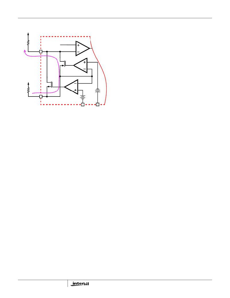
�In� order� to� ensure� the� smooth� transition� of� output� voltage�
�VDIFF�
�during� a� VRM10� VID� change,� a� VID� step� change� smoothing�
�network� is� required� for� an� ISL6566A� based� voltage� regulator.�
�-�
�V� OFS�
�+�
�R� FB�
�FB�
�VREF�
�E/A�
�This� network� is� composed� of� a� 1k� ?� internal� resistor� between�
�the� output� of� DAC� and� the� capacitor� C� REF� ,� between� the� REF�
�pin� and� ground.� The� selection� of� C� REF� is� based� on� the� time�
�duration� for� 1� bit� VID� change� and� the� allowable� delay� time.�
�I� OFS�
�Assuming� the� microprocessor� controls� the� VID� change� at� 1�
�bit� every� T� VID� ,� the� relationship� between� C� REF� and� T� VID� is�
�given� by� Equation� 10.�
�C� REF� =� 0.004X� T� VID�
�(EQ.� 10)�
�VCC�
�As� an� example,� for� a� VID� step� change� rate� of� 5� μ� s� per� bit,� the�
�R� OFS�
�OFS�
�ISL6566A�
�+�
�-�
�0.5V�
�-�
�+�
�1.5V�
�value� of� C� REF� is� 22nF� based� on� Equation� 10.�
�When� running� in� VRM9� or� AMD� Hammer� operation,� the�
�ISL6566A� responds� slightly� different� to� a� dynamic� VID� change�
�than� when� in� VRM10� mode.� In� these� modes� the� VID� code� can�
�GND�
�VCC�
�be� changed� by� more� than� a� 1-bit� step� at� a� time.� Once� the�
�controller� receives� the� new� VID� code� it� waits� half� of� a� phase�
�FIGURE� 9.� NEGATIVE� OFFSET� OUTPUT� VOLTAGE�
�PROGRAMMING�
�Once� the� desired� output� offset� voltage� has� been� determined,�
�use� the� following� formulas� to� set� R� OFS� :�
�cycle� and� then� begins� slewing� the� DAC� 12.5mV� every� phase�
�cycle,� until� the� VID� and� DAC� are� equal.� Thus,� the� total� time�
�required� for� a� VID� change,� t� DVID� ,� is� dependent� on� the� switching�
�frequency� (f� S� ),� the� size� of� the� change� (� ?� V� VID� ),� and� the� time�
�required� to� register� the� VID� change.� The� one-cycle� addition� in�
�0.5� � R� FB�
�V� OFFSET�
�1.5� � R� FB�
�V� OFFSET�
�t� DVID� =� -----� ?� ------------------� +� 1.5� ?�
�f� S� ?� 0.0125�
�For� Positive� Offset� (connect� R� OFS� to� GND):�
�R� OFS� =� --------------------------�
�For� Negative� Offset� (connect� R� OFS� to� VCC):�
�R� OFS� =� --------------------------�
�(EQ.� 8)�
�(EQ.� 9)�
�the� t� DVID� equation� is� due� to� the� possibility� that� the� VID� code�
�change� may� occur� up� to� one� full� switching� cycle� before� being�
�recognized.� The� approximate� time� required� for� a� ISL6566A-�
�based� converter� in� AMD� Hammer� configuration� running� at� f� S� =�
�335kHz� to� make� a� 1.1V� to� 1.5V� reference� voltage� change� is�
�about� 100� μ� s,� as� calculated� using� the� following� equation.�
�1� ?� V� VID� (EQ.� 11)�
�?�
�Dynamic� VID�
�Modern� microprocessors� need� to� make� changes� to� their� core�
�voltage� as� part� of� normal� operation.� They� direct� the� core-�
�voltage� regulator� to� do� this� by� making� changes� to� the� VID�
�inputs.� The� core-voltage� regulator� is� required� to� monitor� the�
�DAC� inputs� and� respond� to� on-the-fly� VID� changes� in� a�
�controlled� manner,� supervising� a� safe� output� voltage� transition�
�without� discontinuity� or� disruption.�
�The� DAC� mode� the� ISL6566A� is� operating� in� determines�
�how� the� controller� responds� to� a� dynamic� VID� change.� When�
�in� VRM10� mode� the� ISL6566A� checks� the� VID� inputs� six�
�times� every� switching� cycle.� If� a� new� code� is� established� and�
�it� stays� the� same� for� 3� consecutive� readings,� the� ISL6566A�
�recognizes� the� change� and� increments� the� reference.�
�Specific� to� VRM10,� the� processor� controls� the� VID�
�transitions� and� is� responsible� for� incrementing� or�
�decrementing� one� VID� step� at� a� time.� In� VRM10� setting,� the�
�ISL6566A� will� immediately� change� the� reference� to� the� new�
�requested� value� as� soon� as� the� request� is� validated;� in�
�cases� where� the� reference� step� is� too� large,� the� sudden�
�change� can� trigger� overcurrent� or� overvoltage� events.�
�15�
�Advanced� Adaptive� Zero� Shoot-Through� Deadtime�
�Control� (Patent� Pending)�
�The� integrated� drivers� incorporate� a� unique� adaptive� deadtime�
�control� technique� to� minimize� deadtime,� resulting� in� high�
�efficiency� from� the� reduced� freewheeling� time� of� the� lower�
�MOSFET� body-diode� conduction,� and� to� prevent� the� upper� and�
�lower� MOSFETs� from� conducting� simultaneously.� This� is�
�accomplished� by� ensuring� either� rising� gate� turns� on� its�
�MOSFET� with� minimum� and� sufficient� delay� after� the� other� has�
�turned� off.�
�During� turn-off� of� the� lower� MOSFET,� the� PHASE� voltage� is�
�monitored� until� it� reaches� a� -0.3V/+0.8V� trip� point� for� a�
�forward/reverse� current,� at� which� time� the� UGATE� is� released�
�to� rise.� An� auto-zero� comparator� is� used� to� correct� the� r� DS(ON)�
�drop� in� the� phase� voltage� preventing� false� detection� of� the�
�-0.3V� phase� level� during� r� DS(ON� conduction� period.� In� the� case�
�of� zero� current,� the� UGATE� is� released� after� 35ns� delay� of� the�
�LGATE� dropping� below� 0.5V.� During� the� phase� detection,� the�
�disturbance� of� LGATE� falling� transition� on� the� PHASE� node� is�
�blanked� out� to� prevent� falsely� tripping.� Once� the� PHASE� is�
�high,� the� advanced� adaptive� shoot-through� circuitry� monitors�
�FN9200.2�
�July� 27,� 2005�
�相关PDF资料 |
PDF描述 |
|---|---|
| ISL6566CRZ-T | IC CTLR PWM BUCK 3PHASE 40-QFN |
| ISL6567CRZ | IC REG CTRLR BUCK PWM VM 24-QFN |
| ISL6568CRZ-T | IC CTLR PWM BUCK 2PHASE 32-QFN |
| ISL6569ACR-T | IC REG CTRLR BUCK PWM 32-QFN |
| ISL6569CR-T | IC REG CTRLR DIVIDER PWM 32-QFN |
相关代理商/技术参数 |
参数描述 |
|---|---|
| ISL6566AIRZ-T | 功能描述:IC CTRLR PWM 3PHASE BUCK 40-QFN RoHS:是 类别:集成电路 (IC) >> PMIC - 稳压器 - 专用型 系列:- 标准包装:43 系列:- 应用:控制器,Intel VR11 输入电压:5 V ~ 12 V 输出数:1 输出电压:0.5 V ~ 1.6 V 工作温度:-40°C ~ 85°C 安装类型:表面贴装 封装/外壳:48-VFQFN 裸露焊盘 供应商设备封装:48-QFN(7x7) 包装:管件 |
| ISL6566CR | 功能描述:IC CTRLR PWM BUCK 3PHASE 40-QFN RoHS:否 类别:集成电路 (IC) >> PMIC - 稳压器 - 专用型 系列:- 产品培训模块:Lead (SnPb) Finish for COTS Obsolescence Mitigation Program 标准包装:2,000 系列:- 应用:电源,ICERA E400,E450 输入电压:4.1 V ~ 5.5 V 输出数:10 输出电压:可编程 工作温度:-40°C ~ 85°C 安装类型:表面贴装 封装/外壳:42-WFBGA,WLCSP 供应商设备封装:42-WLP 包装:带卷 (TR) |
| ISL6566CRR5184 | 制造商:Rochester Electronics LLC 功能描述: 制造商:Intersil Corporation 功能描述: |
| ISL6566CR-T | 功能描述:IC CTRLR PWM BUCK 3PHASE 40-QFN RoHS:否 类别:集成电路 (IC) >> PMIC - 稳压器 - 专用型 系列:- 产品培训模块:Lead (SnPb) Finish for COTS Obsolescence Mitigation Program 标准包装:2,000 系列:- 应用:电源,ICERA E400,E450 输入电压:4.1 V ~ 5.5 V 输出数:10 输出电压:可编程 工作温度:-40°C ~ 85°C 安装类型:表面贴装 封装/外壳:42-WFBGA,WLCSP 供应商设备封装:42-WLP 包装:带卷 (TR) |
| ISL6566CRZ | 功能描述:IC CTRLR PWM BUCK 3PHASE 40QFN RoHS:是 类别:集成电路 (IC) >> PMIC - 稳压器 - 专用型 系列:- 产品培训模块:Lead (SnPb) Finish for COTS Obsolescence Mitigation Program 标准包装:2,000 系列:- 应用:电源,ICERA E400,E450 输入电压:4.1 V ~ 5.5 V 输出数:10 输出电压:可编程 工作温度:-40°C ~ 85°C 安装类型:表面贴装 封装/外壳:42-WFBGA,WLCSP 供应商设备封装:42-WLP 包装:带卷 (TR) |
发布紧急采购,3分钟左右您将得到回复。