参数资料
| 型号: | ISL6568CRZ-T |
| 厂商: | Intersil |
| 文件页数: | 10/30页 |
| 文件大小: | 0K |
| 描述: | IC CTLR PWM BUCK 2PHASE 32-QFN |
| 标准包装: | 1 |
| 应用: | 控制器,Intel VRM9,VRM10,AMD Hammer 应用 |
| 输入电压: | 3 V ~ 12 V |
| 输出数: | 1 |
| 输出电压: | 0.84 V ~ 1.6 V |
| 工作温度: | 0°C ~ 70°C |
| 安装类型: | 表面贴装 |
| 封装/外壳: | 32-VFQFN 裸露焊盘 |
| 供应商设备封装: | 32-QFN(5x5) |
| 包装: | 标准包装 |
| 其它名称: | ISL6568CRZ-TDKR |
第1页第2页第3页第4页第5页第6页第7页第8页第9页当前第10页第11页第12页第13页第14页第15页第16页第17页第18页第19页第20页第21页第22页第23页第24页第25页第26页第27页第28页第29页第30页
�� �
�
�ISL6568�
�(� V� IN� –� V� OUT� )� V� OUT� (EQ.� 1)�
�Interleaving�
�The� switching� of� each� channel� in� a� multi-phase� converter� is�
�timed� to� be� symmetrically� out� of� phase� with� each� of� the� other�
�channels.� In� a� 3-phase� converter,� each� channel� switches� 1/3�
�cycle� after� the� previous� channel� and� 1/3� cycle� before� the�
�following� channel.� As� a� result,� the� three-phase� converter� has� a�
�combined� ripple� frequency� three� times� greater� than� the� ripple�
�frequency� of� any� one� phase.� In� addition,� the� peak-to-peak�
�amplitude� of� the� combined� inductor� currents� is� reduced� in�
�proportion� to� the� number� of� phases� (Equations� 1� and� 2).�
�Increased� ripple� frequency� and� lower� ripple� amplitude� mean�
�that� the� designer� can� use� less� per-channel� inductance� and�
�lower� total� output� capacitance� for� any� performance�
�specification.�
�Figure� 1� illustrates� the� multiplicative� effect� on� output� ripple�
�frequency.� The� three� channel� currents� (IL1,� IL2,� and� IL3)�
�combine� to� form� the� AC� ripple� current� and� the� DC� load� current.�
�The� ripple� component� has� three� times� the� ripple� frequency� of�
�each� individual� channel� current.� Each� PWM� pulse� is� terminated�
�1/3� of� a� cycle� after� the� PWM� pulse� of� the� previous� phase.� The�
�peak-to-peak� current� for� each� phase� is� about� 7A,� and� the� DC�
�components� of� the� inductor� currents� combine� to� feed� the� load.�
�To� understand� the� reduction� of� ripple� current� amplitude� in� the�
�multi-phase� circuit,� examine� the� equation� representing� an�
�individual� channel� peak-to-peak� inductor� current.�
�I� P-P� =� ------------------------------------------------------�
�L� f� S� V� IN�
�In� Equation� 1,� V� IN� and� V� OUT� are� the� input� and� output� voltages�
�respectively,� L� is� the� single-channel� inductor� value,� and� f� S� is�
�the� switching� frequency.�
�The� output� capacitors� conduct� the� ripple� component� of� the�
�inductor� current.� In� the� case� of� multi-phase� converters,� the�
�capacitor� current� is� the� sum� of� the� ripple� currents� from� each� of�
�the� individual� channels.� Compare� Equation� 1� to� the� expression�
�for� the� peak-to-peak� current� after� the� summation� of� N�
�symmetrically� phase-shifted� inductor� currents� in� Equation� 2.�
�Peak-to-peak� ripple� current� decreases� by� an� amount�
�proportional� to� the� number� of� channels.� Output-voltage� ripple�
�is� a� function� of� capacitance,� capacitor� equivalent� series�
�resistance� (ESR),� and� inductor� ripple� current.� Reducing� the�
�inductor� ripple� current� allows� the� designer� to� use� fewer� or� less�
�costly� output� capacitors.�
�12V� to� 1.5V� at� 36A.� The� single-phase� converter� has� 11.9A� RMS�
�input� capacitor� current.� The� single-phase� converter� must� use� an�
�input� capacitor� bank� with� twice� the� RMS� current� capacity� as� the�
�equivalent� three-phase� converter.�
�INPUT-CAPACITOR CURRENT, 10A/DIV�
�CHANNEL� 3�
�INPUT� CURRENT�
�10A/DIV�
�CHANNEL� 2�
�INPUT� CURRENT�
�10A/DIV�
�CHANNEL� 1�
�INPUT� CURRENT�
�10A/DIV�
�1� μ� s/DIV�
�FIGURE� 2.� CHANNEL� INPUT� CURRENTS� AND� INPUT-CAPACITOR�
�RMS� CURRENT� FOR� 3-PHASE� CONVERTER�
��can� be� used� to� determine� the� input-capacitor� RMS� current�
�based� on� load� current,� duty� cycle,� and� the� number� of� channels.�
�They� are� provided� as� aids� in� determining� the� optimal� input�
�capacitor� solution.�
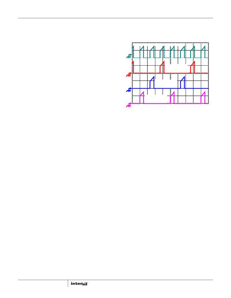
�PWM� Operation�
�The� timing� of� each� converter� leg� is� set� by� the� number� of� active�
�channels.� The� default� channel� setting� for� the� ISL6568� is� two.�
�One� switching� cycle� is� defined� as� the� time� between� the�
�internal� PWM1� pulse� termination� signals.� The� pulse�
�termination� signal� is� the� internally� generated� clock� signal� that�
�triggers� the� falling� edge� of� PWM1.� The� cycle� time� of� the� pulse�
�termination� signal� is� the� inverse� of� the� switching� frequency� set�
�by� the� resistor� between� the� FS� pin� and� ground.� Each� cycle�
�begins� when� the� clock� signal� commands� PWM1� to� go� low.� The�
�PWM1� transition� signals� the� internal� channel-1� MOSFET� driver�
�to� turn� off� the� channel-1� upper� MOSFET� and� turn� on� the�
�channel-1� synchronous� MOSFET.� In� the� default� channel�
�configuration,� the� PWM2� pulse� terminates� 1/2� of� a� cycle� after�
�the� PWM1� pulse.�
�If� the� BOOT2� and� PHASE2� pins� are� both� connected� to� +12V�
�I� C� (� P-P� )� =� ------------------------------------------------------------�
�(� V� IN� –� N� V� OUT� )� V� OUT�
�L� f� S� V� IN�
�(EQ.� 2)�
�single� channel� operation� is� selected.�
�Once� a� PWM� pulse� transitions� low,� it� is� held� low� for� a� minimum�
�of� 1/3� cycle.� This� forced� off� time� is� required� to� ensure� an�
�Another� benefit� of� interleaving� is� to� reduce� input� ripple� current.�
�Input� capacitance� is� determined� in� part� by� the� maximum� input�
�ripple� current.� Multi-phase� topologies� can� improve� overall�
�system� cost� and� size� by� lowering� input� ripple� current� and�
�allowing� the� designer� to� reduce� the� cost� of� input� capacitance.�
�The� example� in� Figure� 2� illustrates� input� currents� from� a�
�three-phase� converter� combining� to� reduce� the� total� input�
�ripple� current.�
�The� converter� depicted� in� Figure� 2� delivers� 1.5V� to� a� 36A� load�
�from� a� 12V� input.� The� RMS� input� capacitor� current� is� 5.9A.�
�Compare� this� to� a� single-phase� converter� also� stepping� down�
�10�
�accurate� current� sample.� Current� sensing� is� described� in� the�
�next� section.� After� the� forced� off� time� expires,� the� PWM� output�
�is� enabled.� The� PWM� output� state� is� driven� by� the� position� of�
�the� error� amplifier� output� signal,� V� COMP� ,� minus� the� current�
�correction� signal� relative� to� the� sawtooth� ramp� as� illustrated� in�
�Figure� 3.� When� the� modified� V� COMP� voltage� crosses� the�
�sawtooth� ramp,� the� PWM� output� transitions� high.� The� internal�
�MOSFET� driver� detects� the� change� in� state� of� the� PWM� signal�
�and� turns� off� the� synchronous� MOSFET� and� turns� on� the� upper�
�MOSFET.� The� PWM� signal� will� remain� high� until� the� pulse�
�termination� signal� marks� the� beginning� of� the� next� cycle� by�
�triggering� the� PWM� signal� low.�
�FN9187.5�
�January� 12,� 2012�
�相关PDF资料 |
PDF描述 |
|---|---|
| ISL6569ACR-T | IC REG CTRLR BUCK PWM 32-QFN |
| ISL6569CR-T | IC REG CTRLR DIVIDER PWM 32-QFN |
| ISL6571CRZ | IC MOSF DRVR/SYNC SW COMPL 68QFN |
| ISL6611AIRZ | IC REG CTRLR DOUBLER PWM 16-QFN |
| ISL6617IRZ | IC PWM DOUBLER MONITOR 10DFN |
相关代理商/技术参数 |
参数描述 |
|---|---|
| ISL6568CRZ-TKR5184 | 功能描述:IC CTRLR PWM 2PHASE BUCK 32-QFN RoHS:是 类别:集成电路 (IC) >> PMIC - 稳压器 - 专用型 系列:- 标准包装:43 系列:- 应用:控制器,Intel VR11 输入电压:5 V ~ 12 V 输出数:1 输出电压:0.5 V ~ 1.6 V 工作温度:-40°C ~ 85°C 安装类型:表面贴装 封装/外壳:48-VFQFN 裸露焊盘 供应商设备封装:48-QFN(7x7) 包装:管件 |
| ISL6568CRZ-TR5184 | 功能描述:IC CTRLR PWM 2PHASE BUCK 32-QFN RoHS:是 类别:集成电路 (IC) >> PMIC - 稳压器 - 专用型 系列:- 标准包装:2,000 系列:- 应用:控制器,DSP 输入电压:4.5 V ~ 25 V 输出数:2 输出电压:最低可调至 1.2V 工作温度:-40°C ~ 85°C 安装类型:表面贴装 封装/外壳:30-TFSOP(0.173",4.40mm 宽) 供应商设备封装:30-TSSOP 包装:带卷 (TR) |
| ISL6568IR | 功能描述:IC CTRLR PWM BUCK 2PHASE 32-QFN RoHS:否 类别:集成电路 (IC) >> PMIC - 稳压器 - 专用型 系列:- 产品培训模块:Lead (SnPb) Finish for COTS Obsolescence Mitigation Program 标准包装:2,000 系列:- 应用:电源,ICERA E400,E450 输入电压:4.1 V ~ 5.5 V 输出数:10 输出电压:可编程 工作温度:-40°C ~ 85°C 安装类型:表面贴装 封装/外壳:42-WFBGA,WLCSP 供应商设备封装:42-WLP 包装:带卷 (TR) |
| ISL6568IR-T | 功能描述:IC CTRLR PWM BUCK 2PHASE 32-QFN RoHS:否 类别:集成电路 (IC) >> PMIC - 稳压器 - 专用型 系列:- 产品培训模块:Lead (SnPb) Finish for COTS Obsolescence Mitigation Program 标准包装:2,000 系列:- 应用:电源,ICERA E400,E450 输入电压:4.1 V ~ 5.5 V 输出数:10 输出电压:可编程 工作温度:-40°C ~ 85°C 安装类型:表面贴装 封装/外壳:42-WFBGA,WLCSP 供应商设备封装:42-WLP 包装:带卷 (TR) |
| ISL6568IRZ | 功能描述:IC CTRLR PWM BUCK 2PHASE 32-QFN RoHS:是 类别:集成电路 (IC) >> PMIC - 稳压器 - 专用型 系列:- 标准包装:43 系列:- 应用:控制器,Intel VR11 输入电压:5 V ~ 12 V 输出数:1 输出电压:0.5 V ~ 1.6 V 工作温度:-40°C ~ 85°C 安装类型:表面贴装 封装/外壳:48-VFQFN 裸露焊盘 供应商设备封装:48-QFN(7x7) 包装:管件 |
发布紧急采购,3分钟左右您将得到回复。