参数资料
| 型号: | ISL6568CRZ-T |
| 厂商: | Intersil |
| 文件页数: | 15/30页 |
| 文件大小: | 0K |
| 描述: | IC CTLR PWM BUCK 2PHASE 32-QFN |
| 标准包装: | 1 |
| 应用: | 控制器,Intel VRM9,VRM10,AMD Hammer 应用 |
| 输入电压: | 3 V ~ 12 V |
| 输出数: | 1 |
| 输出电压: | 0.84 V ~ 1.6 V |
| 工作温度: | 0°C ~ 70°C |
| 安装类型: | 表面贴装 |
| 封装/外壳: | 32-VFQFN 裸露焊盘 |
| 供应商设备封装: | 32-QFN(5x5) |
| 包装: | 标准包装 |
| 其它名称: | ISL6568CRZ-TDKR |
第1页第2页第3页第4页第5页第6页第7页第8页第9页第10页第11页第12页第13页第14页当前第15页第16页第17页第18页第19页第20页第21页第22页第23页第24页第25页第26页第27页第28页第29页第30页
�� �
�
�ISL6568�
�Load-Line� (Droop)� Regulation�
�Some� microprocessor� manufacturers� require� a�
�L�
�V� L� (s)�
�DCR�
�I� OUT�
�precisely-controlled� output� impedance.� This� dependence� of�
�output� voltage� on� load� current� is� often� termed� “droop”� or� “load�
�line”� regulation.�
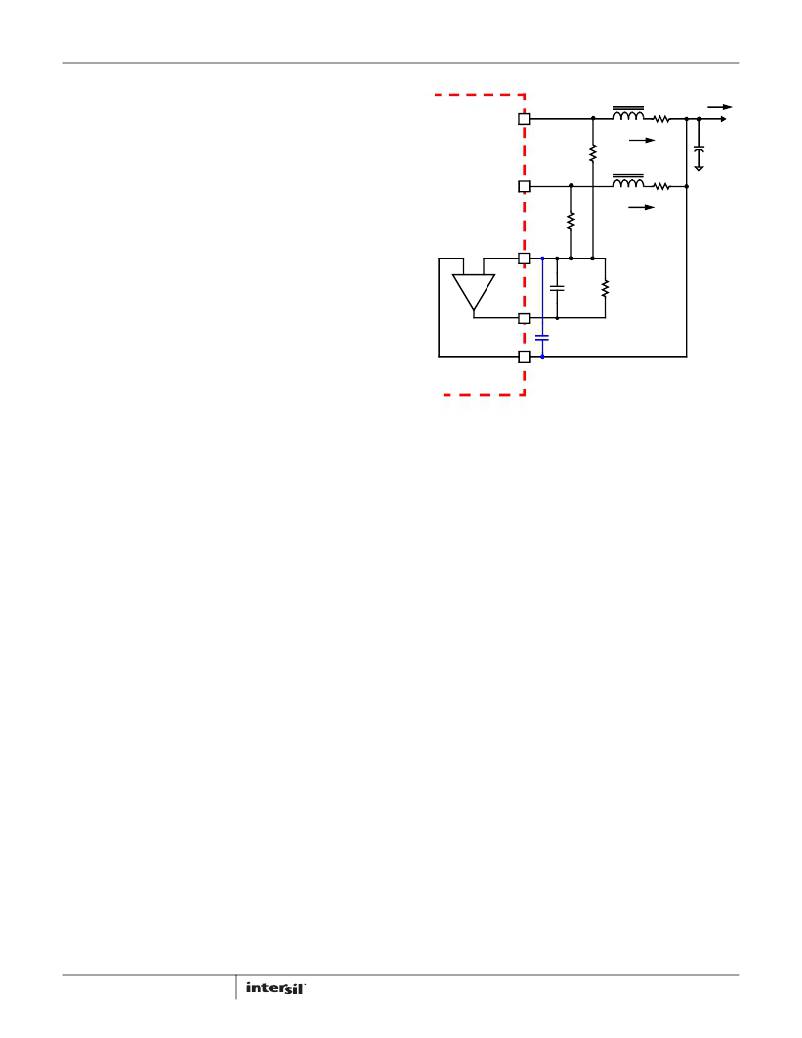
�PHASE1�
�R� S�
�I�
�INDUCTOR�
�L� 1�
�V� OUT�
�C� OUT�
�As� shown� in� Figure� 6,� a� voltage,� V� DROOP� ,� proportional� to� the�
�total� current� in� all� active� channels,� I� OUT� ,� feeds� into� the�
�differential� remote-sense� amplifier.� The� resulting� voltage� at�
�the� output� of� the� remote-sense� amplifier� is� the� sum� of� the�
�output� voltage� and� the� droop� voltage.� Equation� 4� shows� that�
�PHASE2�
�R� S�
�I�
�L�
�DCR�
�INDUCTOR�
�L� 2�
�feeding� this� voltage� into� the� compensation� network� causes� the�
�regulator� to� adjust� the� output� voltage� so� it� will� be� equal� to� the�
�reference� voltage� minus� the� droop� voltage.�
�ISUM�
�The� droop� voltage,� V� DROOP� ,� is� created� by� sensing� the� current�
�through� the� output� inductors.� This� is� accomplished� by� using� a�
�continuous� DCR� current� sensing� method.�
�-�
�ICOMP�
�C� COMP�
�R� COMP�
�Inductor� windings� have� a� characteristic� distributed� resistance�
�or� DCR� (Direct� Current� Resistance).� For� simplicity,� the� inductor�
�V� DROOP�
�+�
�IREF�
�(optional)�
�DCR� is� considered� as� a� separate� lumped� quantity,� as� shown� in�
�Figure� 7.� The� channel� current,� I� L� ,� flowing� through� the� inductor,�
�passes� through� the� DCR.� Equation� 5� shows� the� s-domain�
�equivalent� voltage,� V� L� ,� across� the� inductor.�
�ISL6568�
�FIGURE� 7.� DCR� SENSING� CONFIGURATION�
�V� L� (� s� )� =� I� L� ?� (� s� ?� L� +� DCR� )�
�(EQ.� 5)�
�By� simply� adjusting� the� value� of� R� S� ,� the� load� line� can� be� set� to�
�any� level,� giving� the� converter� the� right� amount� of� droop� at� all�
�(EQ.� 6)�
�?� -------------� +� 1� ?�
�?� DCR� ?�
�COMP�
�(� s� ?� R�
�?� C�
�+� 1� )�
�V� (� s� )� =� --------------------------------------------------------------------------� ?� -----------------------� ?� (� I� +� I� )� ?� DCR�
�V� DROOP� =� ---------------------� ?� I� OUT� ?� DCR�
�The� inductor� DCR� is� important� because� the� voltage� dropped�
�across� it� is� proportional� to� the� channel� current.� By� using� a�
�simple� R-C� network� and� a� current� sense� amplifier,� as� shown� in�
�Figure� 7,� the� voltage� drop� across� all� of� the� inductors’� DCRs� can�
�be� extracted.� The� output� of� the� current� sense� amplifier,�
�V� DROOP� ,� can� be� shown� to� be� proportional� to� the� channel�
�currents� I� L1� and� I� L2� ,� shown� in� Equation� 6.�
�s� ?� L�
�R�
�DROOP� R� L1� L2�
�COMP� COMP� S�
�If� the� R-C� network� components� are� selected� such� that� the� R-C�
�time� constant� matches� the� inductor� L/DCR� time� constant,�
�then� V� DROOP� is� equal� to� the� sum� of� the� voltage� drops� across�
�the� individual� DCRs,� multiplied� by� a� gain.� As� Equation� 7� shows,�
�V� DROOP� is� therefore� proportional� to� the� total� output� current,�
�I� OUT� .�
�R� COMP� (EQ.� 7)�
�R� S�
�15�
�load� currents.� It� may� also� be� necessary� to� compensate� for� any�
�changes� in� DCR� due� to� temperature.� These� changes� cause� the�
�load� line� to� be� skewed,� and� cause� the� R-C� time� constant� to� not�
�match� the� L/DCR� time� constant.� If� this� becomes� a� problem� a�
�simple� negative� temperature� coefficient� resistor� network� can�
�be� used� in� the� place� of� R� COMP� to� compensate� for� the� rise� in�
�DCR� due� to� temperature.�
�Note:� An� optional� 10nF� ceramic� capacitor� from� the� ISUM� pin� to�
�the� IREF� pin� is� recommended� to� help� reduce� any� noise� affects�
�on� the� current� sense� amplifier� due� to� layout.�
�Output-Voltage� Offset� Programming�
�The� ISL6568� allows� the� designer� to� accurately� adjust� the�
�offset� voltage� by� connecting� a� resistor,� R� OFS� ,� from� the� OFS� pin�
�to� VCC� or� GND.� When� R� OFS� is� connected� between� OFS� and�
�VCC,� the� voltage� across� it� is� regulated� to� 1.5V.� This� causes� a�
�proportional� current� (I� OFS� )� to� flow� into� the� OFS� pin� and� out� of�
�the� FB� pin.� If� R� OFS� is� connected� to� ground,� the� voltage� across� it�
�is� regulated� to� 0.5V,� and� I� OFS� flows� into� the� FB� pin� and� out� of�
�the� OFS� pin.� The� offset� current� flowing� through� the� resistor�
�between� VDIFF� and� FB� will� generate� the� desired� offset� voltage�
�which� is� equal� to� the� product� (I� OFS� x� R� FB� ).� These� functions� are�
�shown� in� Figures� 8� and� 9.�
�FN9187.5�
�January� 12,� 2012�
�相关PDF资料 |
PDF描述 |
|---|---|
| ISL6569ACR-T | IC REG CTRLR BUCK PWM 32-QFN |
| ISL6569CR-T | IC REG CTRLR DIVIDER PWM 32-QFN |
| ISL6571CRZ | IC MOSF DRVR/SYNC SW COMPL 68QFN |
| ISL6611AIRZ | IC REG CTRLR DOUBLER PWM 16-QFN |
| ISL6617IRZ | IC PWM DOUBLER MONITOR 10DFN |
相关代理商/技术参数 |
参数描述 |
|---|---|
| ISL6568CRZ-TKR5184 | 功能描述:IC CTRLR PWM 2PHASE BUCK 32-QFN RoHS:是 类别:集成电路 (IC) >> PMIC - 稳压器 - 专用型 系列:- 标准包装:43 系列:- 应用:控制器,Intel VR11 输入电压:5 V ~ 12 V 输出数:1 输出电压:0.5 V ~ 1.6 V 工作温度:-40°C ~ 85°C 安装类型:表面贴装 封装/外壳:48-VFQFN 裸露焊盘 供应商设备封装:48-QFN(7x7) 包装:管件 |
| ISL6568CRZ-TR5184 | 功能描述:IC CTRLR PWM 2PHASE BUCK 32-QFN RoHS:是 类别:集成电路 (IC) >> PMIC - 稳压器 - 专用型 系列:- 标准包装:2,000 系列:- 应用:控制器,DSP 输入电压:4.5 V ~ 25 V 输出数:2 输出电压:最低可调至 1.2V 工作温度:-40°C ~ 85°C 安装类型:表面贴装 封装/外壳:30-TFSOP(0.173",4.40mm 宽) 供应商设备封装:30-TSSOP 包装:带卷 (TR) |
| ISL6568IR | 功能描述:IC CTRLR PWM BUCK 2PHASE 32-QFN RoHS:否 类别:集成电路 (IC) >> PMIC - 稳压器 - 专用型 系列:- 产品培训模块:Lead (SnPb) Finish for COTS Obsolescence Mitigation Program 标准包装:2,000 系列:- 应用:电源,ICERA E400,E450 输入电压:4.1 V ~ 5.5 V 输出数:10 输出电压:可编程 工作温度:-40°C ~ 85°C 安装类型:表面贴装 封装/外壳:42-WFBGA,WLCSP 供应商设备封装:42-WLP 包装:带卷 (TR) |
| ISL6568IR-T | 功能描述:IC CTRLR PWM BUCK 2PHASE 32-QFN RoHS:否 类别:集成电路 (IC) >> PMIC - 稳压器 - 专用型 系列:- 产品培训模块:Lead (SnPb) Finish for COTS Obsolescence Mitigation Program 标准包装:2,000 系列:- 应用:电源,ICERA E400,E450 输入电压:4.1 V ~ 5.5 V 输出数:10 输出电压:可编程 工作温度:-40°C ~ 85°C 安装类型:表面贴装 封装/外壳:42-WFBGA,WLCSP 供应商设备封装:42-WLP 包装:带卷 (TR) |
| ISL6568IRZ | 功能描述:IC CTRLR PWM BUCK 2PHASE 32-QFN RoHS:是 类别:集成电路 (IC) >> PMIC - 稳压器 - 专用型 系列:- 标准包装:43 系列:- 应用:控制器,Intel VR11 输入电压:5 V ~ 12 V 输出数:1 输出电压:0.5 V ~ 1.6 V 工作温度:-40°C ~ 85°C 安装类型:表面贴装 封装/外壳:48-VFQFN 裸露焊盘 供应商设备封装:48-QFN(7x7) 包装:管件 |
发布紧急采购,3分钟左右您将得到回复。