参数资料
| 型号: | ISL6568IR |
| 厂商: | Intersil |
| 文件页数: | 9/30页 |
| 文件大小: | 0K |
| 描述: | IC CTRLR PWM BUCK 2PHASE 32-QFN |
| 标准包装: | 60 |
| 应用: | 控制器,Intel VRM9,VRM10,AMD Hammer 应用 |
| 输入电压: | 3 V ~ 12 V |
| 输出数: | 1 |
| 输出电压: | 0.84 V ~ 1.6 V |
| 工作温度: | -40°C ~ 85°C |
| 安装类型: | 表面贴装 |
| 封装/外壳: | 32-VFQFN 裸露焊盘 |
| 供应商设备封装: | 32-QFN(5x5) |
| 包装: | 管件 |
第1页第2页第3页第4页第5页第6页第7页第8页当前第9页第10页第11页第12页第13页第14页第15页第16页第17页第18页第19页第20页第21页第22页第23页第24页第25页第26页第27页第28页第29页第30页
�� �
�
�ISL6568�
�VSEN� and� RGND�
�VSEN� and� RGND� are� inputs� to� the� precision� differential�
�remote-sense� amplifier� and� should� be� connected� to� the� sense�
�pins� of� the� remote� load.�
�ICOMP,� ISUM,� and� IREF�
�ISUM,� IREF,� and� ICOMP� are� the� DCR� current� sense� amplifier’s�
�negative� input,� positive� input,� and� output� respectively.� For�
�accurate� DCR� current� sensing,� connect� a� resistor� from� each�
�channel’s� phase� node� to� ISUM� and� connect� IREF� to� the�
�summing� point� of� the� output� inductors,� roughly� V� OUT� .� A� parallel�
�R-C� feedback� circuit� connected� between� ISUM� and� ICOMP� will�
�then� create� a� voltage� from� IREF� to� ICOMP� proportional� to� the�
�voltage� drop� across� the� inductor� DCR.� This� voltage� is� referred� to�
�as� the� droop� voltage� and� is� added� to� the� differential�
�remote-sense� amplifier� output.�
�Note:� An� optional� 0.01μF� ceramic� capacitor� can� be� placed�
�from� the� IREF� pin� to� the� ISUM� pin� to� help� reduce� any� noise�
�affects� that� may� occur� due� to� layout.�
�VDIFF�
�VDIFF� is� the� output� of� the� differential� remote-sense� amplifier.�
�The� voltage� on� this� pin� is� equal� to� the� difference� between� VSEN�
�and� RGND� added� to� the� difference� between� IREF� and� ICOMP.�
�VDIFF� therefore� represents� the� output� voltage� plus� the� droop�
�voltage.�
�FB� and� COMP�
�These� pins� are� the� internal� error� amplifier� inverting� input� and�
�output� respectively.� FB,� VDIFF,� and� COMP� are� tied� together�
�through� external� R-C� networks� to� compensate� the� regulator.�
�REF�
�The� REF� input� pin� is� the� positive� input� of� the� error� amplifier.� It� is�
�internally� connected� to� the� DAC� output� through� a� 1k� Ω� resistor.� A�
�capacitor� is� used� between� the� REF� pin� and� ground� to� smooth�
�the� voltage� transition� during� Dynamic� VID� operations.�
�OFS�
�The� OFS� pin� provides� a� means� to� program� a� dc� current� for�
�generating� an� offset� voltage� across� the� resistor� between� FB� and�
�VDIFF.� The� offset� current� is� generated� via� an� external� resistor�
�and� precision� internal� voltage� references.� The� polarity� of� the�
�offset� is� selected� by� connecting� the� resistor� to� GND� or� VCC.� For�
�no� offset,� the� OFS� pin� should� be� left� unconnected.�
�OCSET�
�This� is� the� overcurrent� set� pin.� Placing� a� resistor� from� OCSET� to�
�ICOMP� allows� a� 100� μ� A� current� to� flow� out� this� pin,� producing� a�
�voltage� reference.� Internal� circuitry� compares� the� voltage� at�
�OCSET� to� the� voltage� at� ISUM,� and� if� ISUM� ever� exceeds� OCSET,�
�the� overcurrent� protection� activates.�
�ISEN1� and� ISEN2�
�These� pins� are� used� for� balancing� the� channel� currents� by�
�UGATE1� and� UGATE2�
�Connect� these� pins� to� the� corresponding� upper� MOSFET� gates.�
�These� pins� are� used� to� control� the� upper� MOSFETs� and� are�
�monitored� for� shoot-through� prevention� purposes.� Maximum�
�individual� channel� duty� cycle� is� limited� to� 66%.�
�BOOT1� and� BOOT2�
�These� pins� provide� the� bias� voltage� for� the� corresponding�
�upper� MOSFET� drives.� Connect� these� pins� to�
�appropriately-chosen� external� bootstrap� capacitors.� Internal�
�bootstrap� diodes� connected� to� the� PVCC� pins� provide� the�
�necessary� bootstrap� charge.�
�PHASE1� and� PHASE2�
�Connect� these� pins� to� the� sources� of� the� upper� MOSFETs.�
�These� pins� are� the� return� path� for� the� upper� MOSFET� drives.�
�LGATE1� and� LGATE2�
�These� pins� are� used� to� control� the� lower� MOSFETs.� Connect�
�these� pins� to� the� corresponding� lower� MOSFETs’� gates.�
�PGOOD�
�During� normal� operation� PGOOD� indicates� whether� the� output�
�voltage� is� within� specified� overvoltage� and� undervoltage� limits.�
�If� the� output� voltage� exceeds� these� limits� or� a� reset� event� occurs�
�(such� as� an� overcurrent� event),� PGOOD� is� pulled� low.� PGOOD� is�
�always� low� prior� to� the� end� of� soft-start.�
�Operation�
�Multi-Phase� Power� Conversion�
�Microprocessor� load� current� profiles� have� changed� to� the� point�
�that� the� advantages� of� multi-phase� power� conversion� are�
�impossible� to� ignore.� The� technical� challenges� associated� with�
�producing� a� single-phase� converter� that� is� both� cost-effective�
�and� thermally� viable� have� forced� a� change� to� the� cost-saving�
�approach� of� multi-phase.� The� ISL6568� controller� helps� simplify�
�implementation� by� integrating� vital� functions� and� requiring�
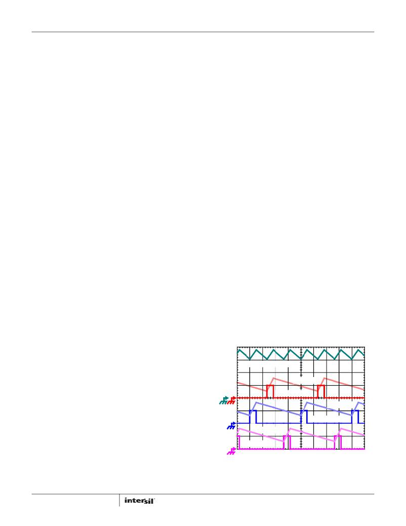
��provides� a� top� level� view� of� multi-phase� power� conversion�
�using� the� ISL6568� controller.�
�IL1� +� IL2� +� IL3,� 7A/DIV�
�IL3,� 7A/DIV�
�PWM3,� 5V/DIV�
�IL2, 7A/DIV�
�PWM2,� 5V/DIV�
�IL1,� 7A/DIV�
�sensing� the� current� through� each� channel’s� lower� MOSFET�
�when� it� is� conducting.� Connect� a� resistor� between� the� ISEN1�
�and� ISEN2� pins� and� their� respective� phase� node.� This� resistor�
�PWM1,� 5V/DIV�
�1� μ� s/DIV�
�sets� a� current� proportional� to� the� current� in� the� lower� MOSFET�
�during� its� conduction� interval.�
�9�
�FIGURE� 1.� PWM� AND� INDUCTOR-CURRENT� WAVEFORMS� FOR�
�3-PHASE� CONVERTER�
�FN9187.5�
�January� 12,� 2012�
�相关PDF资料 |
PDF描述 |
|---|---|
| GMA18DRMD | CONN EDGECARD 36POS .125 SQ WW |
| GCC40DREI-S93 | CONN EDGECARD 80POS .100 EYELET |
| ISL6568CR-T | IC CTRLR PWM BUCK 2PHASE 32-QFN |
| ESM15DTKN | CONN EDGECARD 30POS DIP .156 SLD |
| ISL6568CR | IC CTRLR PWM BUCK 2PHASE 32-QFN |
相关代理商/技术参数 |
参数描述 |
|---|---|
| ISL6568IR-T | 功能描述:IC CTRLR PWM BUCK 2PHASE 32-QFN RoHS:否 类别:集成电路 (IC) >> PMIC - 稳压器 - 专用型 系列:- 产品培训模块:Lead (SnPb) Finish for COTS Obsolescence Mitigation Program 标准包装:2,000 系列:- 应用:电源,ICERA E400,E450 输入电压:4.1 V ~ 5.5 V 输出数:10 输出电压:可编程 工作温度:-40°C ~ 85°C 安装类型:表面贴装 封装/外壳:42-WFBGA,WLCSP 供应商设备封装:42-WLP 包装:带卷 (TR) |
| ISL6568IRZ | 功能描述:IC CTRLR PWM BUCK 2PHASE 32-QFN RoHS:是 类别:集成电路 (IC) >> PMIC - 稳压器 - 专用型 系列:- 标准包装:43 系列:- 应用:控制器,Intel VR11 输入电压:5 V ~ 12 V 输出数:1 输出电压:0.5 V ~ 1.6 V 工作温度:-40°C ~ 85°C 安装类型:表面贴装 封装/外壳:48-VFQFN 裸露焊盘 供应商设备封装:48-QFN(7x7) 包装:管件 |
| ISL6568IRZA | 功能描述:IC CTRLR PWM BUCK 2PHASE 32-QFN RoHS:是 类别:集成电路 (IC) >> PMIC - 稳压器 - 专用型 系列:- 标准包装:43 系列:- 应用:控制器,Intel VR11 输入电压:5 V ~ 12 V 输出数:1 输出电压:0.5 V ~ 1.6 V 工作温度:-40°C ~ 85°C 安装类型:表面贴装 封装/外壳:48-VFQFN 裸露焊盘 供应商设备封装:48-QFN(7x7) 包装:管件 |
| ISL6568IRZA-T | 功能描述:IC CTRLR PWM BUCK 2PHASE 32-QFN RoHS:是 类别:集成电路 (IC) >> PMIC - 稳压器 - 专用型 系列:- 标准包装:43 系列:- 应用:控制器,Intel VR11 输入电压:5 V ~ 12 V 输出数:1 输出电压:0.5 V ~ 1.6 V 工作温度:-40°C ~ 85°C 安装类型:表面贴装 封装/外壳:48-VFQFN 裸露焊盘 供应商设备封装:48-QFN(7x7) 包装:管件 |
| ISL6568IRZR5184 | 功能描述:IC CTRLR PWM 2PHASE BUCK 32-QFN RoHS:是 类别:集成电路 (IC) >> PMIC - 稳压器 - 专用型 系列:- 标准包装:43 系列:- 应用:控制器,Intel VR11 输入电压:5 V ~ 12 V 输出数:1 输出电压:0.5 V ~ 1.6 V 工作温度:-40°C ~ 85°C 安装类型:表面贴装 封装/外壳:48-VFQFN 裸露焊盘 供应商设备封装:48-QFN(7x7) 包装:管件 |
发布紧急采购,3分钟左右您将得到回复。