参数资料
| 型号: | ISL6568IRZA |
| 厂商: | Intersil |
| 文件页数: | 26/30页 |
| 文件大小: | 0K |
| 描述: | IC CTRLR PWM BUCK 2PHASE 32-QFN |
| 标准包装: | 60 |
| 应用: | 控制器,Intel VRM9,VRM10,AMD Hammer 应用 |
| 输入电压: | 3 V ~ 12 V |
| 输出数: | 1 |
| 输出电压: | 0.84 V ~ 1.6 V |
| 工作温度: | -40°C ~ 85°C |
| 安装类型: | 表面贴装 |
| 封装/外壳: | 32-VFQFN 裸露焊盘 |
| 供应商设备封装: | 32-QFN(5x5) |
| 包装: | 管件 |
第1页第2页第3页第4页第5页第6页第7页第8页第9页第10页第11页第12页第13页第14页第15页第16页第17页第18页第19页第20页第21页第22页第23页第24页第25页当前第26页第27页第28页第29页第30页
�� �
�
�ISL6568�
�0.6�
�0.4�
�When� placing� the� MOSFETs� try� to� keep� the� source� of� the� upper�
�FETs� and� the� drain� of� the� lower� FETs� as� close� as� thermally� possible.�
�Input� Bulk� capacitors� should� be� placed� close� to� the� drain� of� the�
�upper� FETs� and� the� source� of� the� lower� FETs.� Locate� the� output�
�inductors� and� output� capacitors� between� the� MOSFETs� and� the� load.�
�The� high-frequency� input� and� output� decoupling� capacitors�
�(ceramic)� should� be� placed� as� close� as� practicable� to� the� decoupling�
�target,� making� use� of� the� shortest� connection� paths� to� any� internal�
�planes,� such� as� vias� to� GND� next� or� on� the� capacitor� solder� pad.�
�0.2�
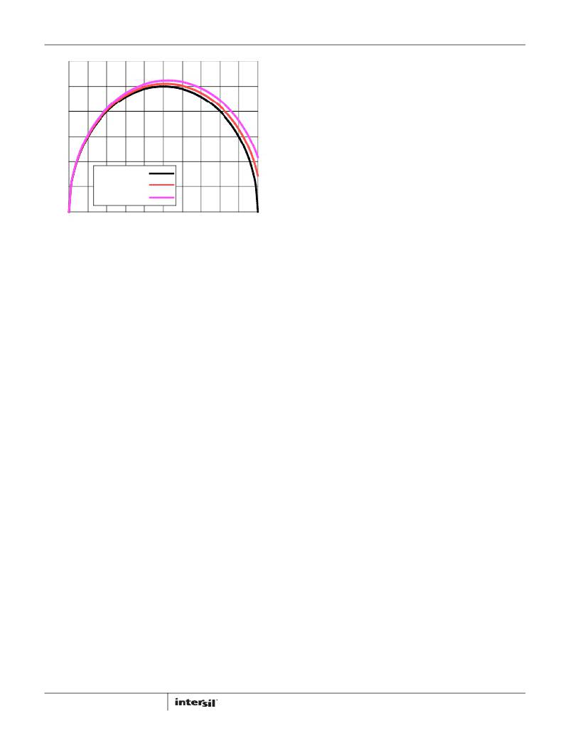
�I� L(P-P)� =� 0�
�I� L(P-P)� =� 0.5� I� O�
�The� critical� small� components� include� the� bypass� capacitors� for�
�VCC� and� PVCC,� and� many� of� the� components� surrounding� the�
�controller� including� the� feedback� network� and� current� sense�
�components.� Locate� the� VCC/PVCC� bypass� capacitors� as� close� to�
�0�
�0�
�I� L(P-P)� =� 0.75� I� O�
�0.2� 0.4�
�0.6�
�0.8�
�1.0�
�the� ISL6566� as� possible.� It� is� especially� important� to� locate� the�
�components� associated� with� the� feedback� circuit� close� to� their�
�respective� controller� pins,� since� they� belong� to� a� high-impedance�
�DUTY� CYCLE� (V� IN� /V� O� )�
�FIGURE� 23.� NORMALIZED� INPUT-CAPACITOR� RMS� CURRENT� FOR�
�SINGLE-PHASE� CONVERTER�
�Low� capacitance,� high-frequency� ceramic� capacitors� are� needed� in�
�addition� to� the� input� bulk� capacitors� to� suppress� leading� and�
�falling� edge� voltage� spikes.� The� spikes� result� from� the� high� current�
�slew� rate� produced� by� the� upper� MOSFET� turn� on� and� off.� Select�
�low� ESL� ceramic� capacitors� and� place� one� as� close� as� possible� to�
�each� upper� MOSFET� drain� to� minimize� board� parasitics� and�
�maximize� suppression.�
�Layout� Considerations�
�MOSFETs� switch� very� fast� and� efficiently.� The� speed� with� which�
�the� current� transitions� from� one� device� to� another� causes� voltage�
�spikes� across� the� interconnecting� impedances� and� parasitic�
�circuit� elements.� These� voltage� spikes� can� degrade� efficiency,�
�radiate� noise� into� the� circuit� and� lead� to� device� overvoltage�
�stress.� Careful� component� selection,� layout,� and� placement�
�minimizes� these� voltage� spikes.� Consider,� as� an� example,� the�
�turnoff� transition� of� the� upper� PWM� MOSFET.� Prior� to� turnoff,� the�
�upper� MOSFET� was� carrying� channel� current.� During� the� turnoff,�
�current� stops� flowing� in� the� upper� MOSFET� and� is� picked� up� by�
�the� lower� MOSFET.� Any� inductance� in� the� switched� current� path�
�generates� a� large� voltage� spike� during� the� switching� interval.�
�Careful� component� selection,� tight� layout� of� the� critical�
�components,� and� short,� wide� circuit� traces� minimize� the�
�magnitude� of� voltage� spikes.�
�There� are� two� sets� of� critical� components� in� a� DC/DC� converter�
�using� a� ISL6566� controller.� The� power� components� are� the� most�
�critical� because� they� switch� large� amounts� of� energy.� Next,� are�
�small� signal� components� that� connect� to� sensitive� nodes� or�
�supply� critical� bypassing� current� and� signal� coupling.�
�The� power� components� should� be� placed� first,� which� include� the�
�MOSFETs,� input� and� output� capacitors,� and� the� inductors.� It� is�
�important� to� have� a� symmetrical� layout� for� each� power� train,�
�preferably� with� the� controller� located� equidistant� from� each.�
�Symmetrical� layout� allows� heat� to� be� dissipated� equally� across� all�
�three� power� trains.� Equidistant� placement� of� the� controller� to� the�
�three� power� trains� also� helps� keep� the� gate� drive� traces� equally�
�short,� resulting� in� equal� trace� impedances� and� similar� drive�
�capability� of� all� sets� of� MOSFETs.�
�26�
�circuit� loop,� sensitive� to� EMI� pick-up.� It� is� also� important� to� place�
�the� current� sense� components� close� to� their� respective� pins� on�
�the� ISL6566,� including� R� ISEN� ,� R� S� ,� R� COMP� ,� and� C� COMP� .�
�A� multi-layer� printed� circuit� board� is� recommended.� Figure� 24� shows�
�the� connections� of� the� critical� components� for� the� converter.� Note�
�that� capacitors� C� xxIN� and� C� xxOUT� could� each� represent� numerous�
�physical� capacitors.� Dedicate� one� solid� layer,� usually� the� one�
�underneath� the� component� side� of� the� board,� for� a� ground� plane�
�and� make� all� critical� component� ground� connections� with� vias� to�
�this� layer.� Dedicate� another� solid� layer� as� a� power� plane� and� break�
�this� plane� into� smaller� islands� of� common� voltage� levels.� Keep� the�
�metal� runs� from� the� PHASE� terminal� to� output� inductors� short.� The�
�power� plane� should� support� the� input� power� and� output� power�
�nodes.� Use� copper� filled� polygons� on� the� top� and� bottom� circuit�
�layers� for� the� phase� nodes.� Use� the� remaining� printed� circuit� layers�
�for� small� signal� wiring.�
�Routing� UGATE,� LGATE,� and� PHASE� Traces�
�Great� attention� should� be� paid� to� routing� the� UGATE,� LGATE,� and�
�PHASE� traces� since� they� drive� the� power� train� MOSFETs� using�
�short,� high� current� pulses.� It� is� important� to� size� them� as� large� and�
�as� short� as� possible� to� reduce� their� overall� impedance� and�
�inductance.� They� should� be� sized� to� carry� at� least� one� ampere� of�
�current� (0.02”� to� 0.05”).� Going� between� layers� with� vias� should� also�
�be� avoided,� but� if� so,� use� two� vias� for� interconnection� when� possible.�
�Extra� care� should� be� given� to� the� LGATE� traces� in� particular� since�
�keeping� their� impedance� and� inductance� low� helps� to� significantly�
�reduce� the� possibility� of� shoot-through.� It� is� also� important� to� route�
�each� channels� UGATE� and� PHASE� traces� in� as� close� proximity� as�
�possible� to� reduce� their� inductances.�
�Thermal� Management�
�For� maximum� thermal� performance� in� high� current,� high�
�switching� frequency� applications,� connecting� the� thermal� GND�
�pad� of� the� ISL6566� to� the� ground� plane� with� multiple� vias� is�
�recommended.� This� heat� spreading� allows� the� part� to� achieve�
�its� full� thermal� potential.� It� is� also� recommended� that� the�
�controller� be� placed� in� a� direct� path� of� airflow� if� possible� to� help�
�thermally� manage� the� part.�
�FN9187.5�
�January� 12,� 2012�
�相关PDF资料 |
PDF描述 |
|---|---|
| ISL6568IRZ | IC CTRLR PWM BUCK 2PHASE 32-QFN |
| GCA49DTMT | CONN EDGECARD 98POS R/A .125 SLD |
| GCA49DTBT | CONN EDGECARD 98POS R/A .125 SLD |
| GCA49DTAT | CONN EDGECARD 98POS R/A .125 SLD |
| ISL6323BCRZ-T | IC PWM CTRLR SYNC BUCK DL 48QFN |
相关代理商/技术参数 |
参数描述 |
|---|---|
| ISL6568IRZA-T | 功能描述:IC CTRLR PWM BUCK 2PHASE 32-QFN RoHS:是 类别:集成电路 (IC) >> PMIC - 稳压器 - 专用型 系列:- 标准包装:43 系列:- 应用:控制器,Intel VR11 输入电压:5 V ~ 12 V 输出数:1 输出电压:0.5 V ~ 1.6 V 工作温度:-40°C ~ 85°C 安装类型:表面贴装 封装/外壳:48-VFQFN 裸露焊盘 供应商设备封装:48-QFN(7x7) 包装:管件 |
| ISL6568IRZR5184 | 功能描述:IC CTRLR PWM 2PHASE BUCK 32-QFN RoHS:是 类别:集成电路 (IC) >> PMIC - 稳压器 - 专用型 系列:- 标准包装:43 系列:- 应用:控制器,Intel VR11 输入电压:5 V ~ 12 V 输出数:1 输出电压:0.5 V ~ 1.6 V 工作温度:-40°C ~ 85°C 安装类型:表面贴装 封装/外壳:48-VFQFN 裸露焊盘 供应商设备封装:48-QFN(7x7) 包装:管件 |
| ISL6568IRZ-T | 功能描述:IC CTRLR PWM BUCK 2PHASE 32-QFN RoHS:是 类别:集成电路 (IC) >> PMIC - 稳压器 - 专用型 系列:- 标准包装:43 系列:- 应用:控制器,Intel VR11 输入电压:5 V ~ 12 V 输出数:1 输出电压:0.5 V ~ 1.6 V 工作温度:-40°C ~ 85°C 安装类型:表面贴装 封装/外壳:48-VFQFN 裸露焊盘 供应商设备封装:48-QFN(7x7) 包装:管件 |
| ISL6568IRZ-TR5184 | 功能描述:IC CTRLR PWM 2PHASE BUCK 32-QFN RoHS:是 类别:集成电路 (IC) >> PMIC - 稳压器 - 专用型 系列:- 标准包装:43 系列:- 应用:控制器,Intel VR11 输入电压:5 V ~ 12 V 输出数:1 输出电压:0.5 V ~ 1.6 V 工作温度:-40°C ~ 85°C 安装类型:表面贴装 封装/外壳:48-VFQFN 裸露焊盘 供应商设备封装:48-QFN(7x7) 包装:管件 |
| ISL6569ACB | 功能描述:IC REG CTRLR BUCK PWM 24-SOIC RoHS:否 类别:集成电路 (IC) >> PMIC - 稳压器 - DC DC 切换控制器 系列:- 标准包装:2,500 系列:- PWM 型:电流模式 输出数:1 频率 - 最大:500kHz 占空比:100% 电源电压:8.2 V ~ 30 V 降压:无 升压:无 回扫:是 反相:无 倍增器:无 除法器:无 Cuk:无 隔离:是 工作温度:0°C ~ 70°C 封装/外壳:8-DIP(0.300",7.62mm) 包装:管件 产品目录页面:1316 (CN2011-ZH PDF) |
发布紧急采购,3分钟左右您将得到回复。