- 您现在的位置:买卖IC网 > PDF目录20645 > ISL6610ACBZ-T (Intersil)IC MOSFET DRVR DUAL SYNC 14-SOIC PDF资料下载
参数资料
| 型号: | ISL6610ACBZ-T |
| 厂商: | Intersil |
| 文件页数: | 8/11页 |
| 文件大小: | 0K |
| 描述: | IC MOSFET DRVR DUAL SYNC 14-SOIC |
| 标准包装: | 2,500 |
| 配置: | 高端和低端,同步 |
| 输入类型: | PWM |
| 延迟时间: | 18ns |
| 配置数: | 2 |
| 输出数: | 4 |
| 高端电压 - 最大(自引导启动): | 36V |
| 电源电压: | 4.5 V ~ 5.5 V |
| 工作温度: | 0°C ~ 70°C |
| 安装类型: | 表面贴装 |
| 封装/外壳: | 14-SOIC(0.154",3.90mm 宽) |
| 供应商设备封装: | 14-SOICN |
| 包装: | 带卷 (TR) |
�� �
�
�ISL6610,� ISL6610A�
�PVCC�
�BOOT�
�C� GD�
�D�
�profile� MOSFETs,� such� as� Direct� FETs� and� multi-SOURCE�
�leads� devices� (SO-8,� LFPAK,� PowerPAK),� have� low� parasitic�
�lead� inductances� and� can� be� driven� by� either� ISL6610� or�
�ISL6610A� (assuming� proper� layout� design).� The� ISL6610,�
�R� HI1�
�R� LO1�
�UGATE�
�G�
�R� G1�
�R� GI1�
�C� GS�
�C� DS�
�Q1�
�missing� the� 3� Ω� integrated� BOOT� resistor,� typically� yields�
�slightly� higher� efficiency� than� the� ISL6610A.�
�Layout� Considerations�
�S�
�PHASE�
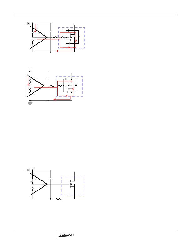
�FIGURE� 3.� TYPICAL� UPPER-GATE� DRIVE� TURN-ON� PATH�
�PVCC�
�D�
�A� good� layout� helps� reduce� the� ringing� on� the� switching�
�node� (PHASE)� and� significantly� lower� the� stress� applied� to�
�the� output� drives.� The� following� advice� is� meant� to� lead� to� an�
�optimized� layout� and� performance:�
�?� Keep� decoupling� loops� (VCC-GND,� PVCC-PGND� and�
�BOOT-PHASE)� short� and� wide,� at� least� 25� mils.� Avoid�
�using� vias� on� decoupling� components� other� than� their�
�R� HI2�
�R� LO2�
�LGATE�
�GND�
�G�
�R� G2�
�C� GD�
�R� GI2�
�C� GS�
�S�
�C� DS�
�Q2�
�ground� terminals,� which� should� be� on� a� copper� plane� with�
�at� least� two� vias.�
�?� Minimize� trace� inductance,� especially� on� low-impedance�
�lines.� All� power� traces� (UGATE,� PHASE,� LGATE,� PGND,�
�PVCC,� VCC,� GND)� should� be� short� and� wide,� at� least� 25�
�mils.� Try� to� place� power� traces� on� a� single� layer,�
�otherwise,� two� vias� on� interconnection� are� preferred�
�where� possible.� For� no� connection� (NC)� pins� on� the� QFN�
�FIGURE� 4.� TYPICAL� LOWER-GATE� DRIVE� TURN-ON� PATH�
�Application� Information�
�MOSFET� and� Driver� Selection�
�The� parasitic� inductances� of� the� PCB� and� of� the� power�
�devices’� packaging� (both� upper� and� lower� MOSFETs)� can�
�cause� serious� ringing,� exceeding� absolute� maximum� rating�
�of� the� devices.� The� negative� ringing� at� the� edges� of� the�
�PHASE� node� could� increase� the� bootstrap� capacitor� voltage�
�through� the� internal� bootstrap� diode,� and� in� some� cases,� it�
�may� overstress� the� upper� MOSFET� driver.� Careful� layout,�
�proper� selection� of� MOSFETs� and� packaging,� as� well� as� the�
�proper� driver� can� go� a� long� way� toward� minimizing� such�
�unwanted� stress.�
�part,� connect� it� to� the� adjacent� net� (LGATE2/PHASE2)� can�
�reduce� trace� inductance.�
�?� Shorten� all� gate� drive� loops� (UGATE-PHASE� and� LGATE-�
�PGND)� and� route� them� closely� spaced.�
�?� Minimize� the� inductance� of� the� PHASE� node.� Ideally,� the�
�source� of� the� upper� and� the� drain� of� the� lower� MOSFET�
�should� be� as� close� as� thermally� allowable.�
�?� Minimize� the� current� loop� of� the� output� and� input� power�
�trains.� Short� the� source� connection� of� the� lower� MOSFET�
�to� ground� as� close� to� the� transistor� pin� as� feasible.� Input�
�capacitors� (especially� ceramic� decoupling)� should� be�
�placed� as� close� to� the� drain� of� upper� and� source� of� lower�
�MOSFETs� as� possible.�
�?� Avoid� routing� relatively� high� impedance� nodes� (such� as�
�PWM� and� ENABLE� lines)� close� to� high� dV/dt� UGATE� and�
�PHASE� nodes.�
�PVCC�
�BOOT�
�D�
�In� addition,� connecting� the� thermal� pad� of� the� QFN� package�
�to� the� power� ground� through� multiple� vias,� or� placing� a� low�
�noise� copper� plane� (such� as� power� ground)� underneath� the�
�R� HI1�
�G�
�SOIC� part� is� recommended.� This� is� to� improve� heat�
�R� LO1�
�UGATE�
�Q1�
�dissipation� and� allow� the� part� to� achieve� its� full� thermal�
�potential.�
�R� PH� =1-2� Ω�
�S�
�PHASE�
�FIGURE� 5.� PHASE� RESISTOR� TO� MINIMIZE� SERIOUS�
�NEGATIVE� PHASE� SPIKE�
�The� selection� of� D� 2� -PAK,� or� D-PAK� packaged� MOSFETs,� is�
�a� much� better� match� (for� the� reasons� discussed)� for� the�
�ISL6610A� with� a� phase� resistor,� as� shown� in� Figure� 5.� Low-�
�8�
�Upper� MOSFET� Self� Turn-On� Effects� At� Startup�
�Should� the� driver� have� insufficient� bias� voltage� applied,� its�
�outputs� are� floating.� If� the� input� bus� is� energized� at� a� high�
�dV/dt� rate� while� the� driver� outputs� are� floating,� due� to� the�
�self-coupling� via� the� internal� C� GD� of� the� MOSFET,� the�
�UGATE� could� momentarily� rise� up� to� a� level� greater� than� the�
�threshold� voltage� of� the� MOSFET.� This� could� potentially� turn�
�on� the� upper� switch� and� result� in� damaging� inrush� energy.�
�FN6395.0�
�November� 22,� 2006�
�相关PDF资料 |
PDF描述 |
|---|---|
| GBC05DRTS-S93 | CONN EDGECARD 10POS DIP .100 SLD |
| ACM36DSAN | CONN EDGECARD 72POS R/A .156 SLD |
| GBM22DSES-S243 | CONN EDGECARD 44POS .156 EYELET |
| NMN0.50BK100 | NYLON MULTI 1/2" BLACK 100' |
| VI-J5D-CX-F4 | CONVERTER MOD DC/DC 85V 75W |
相关代理商/技术参数 |
参数描述 |
|---|---|
| ISL6610ACRZ | 功能描述:IC MOSFET DRVR DUAL SYNC 16-QFN RoHS:是 类别:集成电路 (IC) >> PMIC - MOSFET,电桥驱动器 - 外部开关 系列:- 标准包装:50 系列:- 配置:高端 输入类型:非反相 延迟时间:200ns 电流 - 峰:250mA 配置数:1 输出数:1 高端电压 - 最大(自引导启动):600V 电源电压:12 V ~ 20 V 工作温度:-40°C ~ 125°C 安装类型:通孔 封装/外壳:8-DIP(0.300",7.62mm) 供应商设备封装:8-DIP 包装:管件 其它名称:*IR2127 |
| ISL6610ACRZ-T | 功能描述:IC MOSFET DRVR DUAL SYNC 16-QFN RoHS:是 类别:集成电路 (IC) >> PMIC - MOSFET,电桥驱动器 - 外部开关 系列:- 标准包装:6,000 系列:* |
| ISL6610AIBZ | 功能描述:IC MOSFET DRVR DUAL SYNC 14-SOIC RoHS:是 类别:集成电路 (IC) >> PMIC - MOSFET,电桥驱动器 - 外部开关 系列:- 标准包装:50 系列:- 配置:高端 输入类型:非反相 延迟时间:200ns 电流 - 峰:250mA 配置数:1 输出数:1 高端电压 - 最大(自引导启动):600V 电源电压:12 V ~ 20 V 工作温度:-40°C ~ 125°C 安装类型:通孔 封装/外壳:8-DIP(0.300",7.62mm) 供应商设备封装:8-DIP 包装:管件 其它名称:*IR2127 |
| ISL6610AIBZ-T | 功能描述:IC MOSFET DRVR DUAL SYNC 14-SOIC RoHS:是 类别:集成电路 (IC) >> PMIC - MOSFET,电桥驱动器 - 外部开关 系列:- 标准包装:6,000 系列:* |
| ISL6610AIRZ | 功能描述:IC MOSFET DRVR DUAL SYNC 16-QFN RoHS:是 类别:集成电路 (IC) >> PMIC - MOSFET,电桥驱动器 - 外部开关 系列:- 标准包装:50 系列:- 配置:高端 输入类型:非反相 延迟时间:200ns 电流 - 峰:250mA 配置数:1 输出数:1 高端电压 - 最大(自引导启动):600V 电源电压:12 V ~ 20 V 工作温度:-40°C ~ 125°C 安装类型:通孔 封装/外壳:8-DIP(0.300",7.62mm) 供应商设备封装:8-DIP 包装:管件 其它名称:*IR2127 |
发布紧急采购,3分钟左右您将得到回复。