- 您现在的位置:买卖IC网 > PDF目录20645 > ISL6620IRZ (Intersil)IC SYNC RECT MOSFET DRVR 10-DFN PDF资料下载
参数资料
| 型号: | ISL6620IRZ |
| 厂商: | Intersil |
| 文件页数: | 7/10页 |
| 文件大小: | 0K |
| 描述: | IC SYNC RECT MOSFET DRVR 10-DFN |
| 标准包装: | 100 |
| 配置: | 高端和低端,同步 |
| 输入类型: | PWM |
| 延迟时间: | 40ns |
| 电流 - 峰: | 2A |
| 配置数: | 1 |
| 输出数: | 2 |
| 高端电压 - 最大(自引导启动): | 36V |
| 电源电压: | 4.5 V ~ 5.5 V |
| 工作温度: | -40°C ~ 85°C |
| 安装类型: | 表面贴装 |
| 封装/外壳: | 10-VFDFN 裸露焊盘 |
| 供应商设备封装: | 10-DFN(3x3) |
| 包装: | 管件 |
| 产品目录页面: | 1248 (CN2011-ZH PDF) |
�� �
�
�ISL6620,� ISL6620A�
�Power-On� Reset� (POR)� Function�
�During� initial� start-up,� the� VCC� voltage� rise� is� monitored.� Once�
�the� rising� VCC� voltage� exceeds� 3.8V� (typically),� operation� of�
�the� driver� is� enabled� and� the� PWM� input� signal� takes� control�
�improvement� suggestions.� The� total� gate� drive� power� losses�
�due� to� the� gate� charge� of� MOSFETs� and� the� driver’s� internal�
�circuitry� and� their� corresponding� average� driver� current� can�
�be� estimated� using� Equations� 2� and� 3,� respectively:�
�of� the� gate� drives.� If� VCC� drops� below� the� falling� threshold� of�
�3.5V� (typically),� operation� of� the� driver� is� disabled.�
�P� Qg_TOT� =� P� Qg_Q1� +� P� Qg_Q2� +� I� Q� ?� VCC�
�(EQ.� 2)�
�P� Qg_Q1� =� ---------------------------------------� ?� F� SW� ?� N� Q1�
�P� Qg_Q2� =� --------------------------------------� ?� F� SW� ?� N� Q2�
�?� Q� G1� ?� UVCC� ?� N� Q1� Q� G2� ?� LVCC� ?� N� Q2� ?�
�I� DR� =� ?� ------------------------------------------------------� +� -----------------------------------------------------� ?� ?� F� SW� +� I� Q�
�Internal� Bootstrap� Device�
�ISL6620,� ISL6620A� features� an� internal� bootstrap� Schottky�
�diode.� Simply� adding� an� external� capacitor� across� the� BOOT�
�and� PHASE� pins� completes� the� bootstrap� circuit.� The�
�bootstrap� function� is� also� designed� to� prevent� the� bootstrap�
�capacitor� from� overcharging� due� to� the� large� negative� swing�
�at� the� trailing-edge� of� the� PHASE� node.� This� reduces�
�voltage� stress� on� the� BOOT� to� PHASE� pins.�
�1.6�
�1.4�
�1.2�
�1.0�
�0.8�
�0.6�
�Q� GATE� = 100nC�
�0.4�
�Q� G1� ?� UVCC� 2�
�V� GS1�
�Q� G2� ?� LVCC� 2�
�V� GS2�
�?� V� GS1� V� GS2� ?�
�(EQ.� 3)�
�where� the� gate� charge� (Q� G1� and� Q� G2� )� is� defined� at� a�
�particular� gate� to� source� voltage� (V� GS1� and� V� GS2� )� in� the�
�corresponding� MOSFET� data� sheet;� I� Q� is� the� driver� ’s� total�
�quiescent� current� with� no� load� at� both� drive� outputs;� N� Q1�
�and� N� Q2� are� number� of� upper� and� lower� MOSFETs,�
�respectively;� UVCC� and� LVCC� are� the� drive� voltages� for�
�both� upper� and� lower� FETs,� respectively.� The� I� Q*� VCC�
�product� is� the� quiescent� power� of� the� driver� without� a� load.�
�0.2�
�20nC�
�50nC�
�P� DR� =� P� DR_UP� +� P� DR_LOW� +� I� Q� ?� VCC�
�(EQ.� 4)�
�P� DR_UP� =� ?� --------------------------------------� +� ----------------------------------------� ?� ?� ---------------------�
�?� R� HI1� +� R� EXT1� R� LO1� +� R� EXT1� ?�
�0.0�
�0.0�
�0.1�
�0.2�
�0.3�
�0.4� 0.5� 0.6�
�Δ� V� BOOT_CAP� (V)�
�0.7�
�0.8�
�0.9�
�1.0�
�?� R� HI1� R� LO1� ?� P� Qg_Q1�
�2�
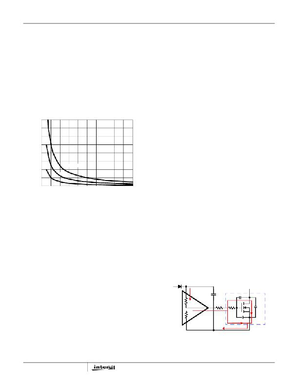
�FIGURE� 2.� BOOTSTRAP� CAPACITANCE� vs� BOOT� RIPPLE�
�P� DR_LOW� =� ?� --------------------------------------� +� ----------------------------------------� ?� ?� ---------------------�
�?� R� HI2� +� R� EXT2� R� LO2� +� R� EXT2� ?�
�C� BOOT_CAP� ≥� --------------------------------------�
�Δ� V� BOOT_CAP�
�R� EXT1� =� R� G1� +� -------------� R� EXT2� =� R� G2� +� -------------�
�N� N�
�Q� GATE� =� -------------------------------� ?� N� Q1�
�VOLTAGE�
�The� bootstrap� capacitor� must� have� a� maximum� voltage�
�rating� well� above� the� maximum� voltage� intended� for� VCC.� Its�
�capacitance� value� can� be� estimated� using� Equation� 1:�
�Q� GATE�
�(EQ.� 1)�
�Q� G1� ?� VCC�
�V� GS1�
�where� Q� G1� is� the� amount� of� gate� charge� per� upper� MOSFET�
�at� V� GS1� gate-source� voltage� and� N� Q1� is� the� number� of�
�control� MOSFETs.� The� Δ� V� BOOT_CAP� term� is� defined� as� the�
�allowable� droop� in� the� rail� of� the� upper� gate� drive.� Select�
�?� R� HI2� R� LO2� ?� P� Qg_Q2�
�2�
�R� GI1� R� GI2�
�Q1� Q2�
�The� total� gate� drive� power� losses� are� dissipated� among� the�
�resistive� components� along� the� transition� path,� as� outlined� in�
�Equation� 4.� The� drive� resistance� dissipates� a� portion� of� the�
�total� gate� drive� power� losses,� the� rest� will� be� dissipated� by� the�
�external� gate� resistors� (R� G1� and� R� G2� )� and� the� internal� gate�
�resistors� (R� GI1� and� R� GI2� )� of� MOSFETs.� Figures� 3� and� 4� show�
�the� typical� upper� and� lower� gate� drives� turn-on� current� paths.�
�results� are� exemplified� in� Figure� 2.�
�UVCC�
�BOOT�
�Power� Dissipation�
�Package� power� dissipation� is� mainly� a� function� of� the�
�switching� frequency� (F� SW� ),� the� output� drive� impedance,� the�
�layout� resistance,� and� the� selected� MOSFET’s� internal� gate�
�resistance� and� total� gate� charge� (Q� G� ).� Calculating� the� power�
�dissipation� in� the� driver� for� a� desired� application� is� critical� to�
�ensure� safe� operation.� Exceeding� the� maximum� allowable�
�R� HI1�
�R� LO1�
�G�
�R� L1�
�C� GD�
�R� G1�
�C� GS�
�S�
�D�
�C� DS�
�Q1�
�power� dissipation� level� may� push� the� IC� beyond� the� maximum�
�recommended� operating� junction� temperature.� The� DFN�
�package� is� more� suitable� for� high� frequency� applications.� See�
�“Layout� Considerations”� on� page� 8� for� thermal� impedance�
�7�
�PHASE�
�FIGURE� 3.� TYPICAL� UPPER-GATE� DRIVE� TURN-ON� PATH�
�FN6494.0�
�April� 25,� 2008�
�相关PDF资料 |
PDF描述 |
|---|---|
| NMN0.75BK75 | NYLON MULTI 3/4" BLACK 75' |
| MBR2535CTG | DIODE SCHOTTKY 35V 30A TO220AB |
| T95Z336K016CSSL | CAP TANT 33UF 16V 10% 2910 |
| ABM43DRMH | CONN EDGECARD 86POS .156 WW |
| EEM18DRMT-S288 | CONN EDGECARD 36POS .156 EXTEND |
相关代理商/技术参数 |
参数描述 |
|---|---|
| ISL6620IRZ-T | 功能描述:IC MOSFET DVR SYNC BUCK 10-DFN RoHS:是 类别:集成电路 (IC) >> PMIC - MOSFET,电桥驱动器 - 外部开关 系列:- 标准包装:6,000 系列:* |
| ISL6622ACBZ | 功能描述:IC MOSFET DRVR SYNC BUCK 8-SOIC RoHS:是 类别:集成电路 (IC) >> PMIC - MOSFET,电桥驱动器 - 外部开关 系列:- 标准包装:50 系列:- 配置:高端 输入类型:非反相 延迟时间:200ns 电流 - 峰:250mA 配置数:1 输出数:1 高端电压 - 最大(自引导启动):600V 电源电压:12 V ~ 20 V 工作温度:-40°C ~ 125°C 安装类型:通孔 封装/外壳:8-DIP(0.300",7.62mm) 供应商设备封装:8-DIP 包装:管件 其它名称:*IR2127 |
| ISL6622ACBZ-T | 功能描述:IC MOSFET DRVR SYNC BUCK 8-SOIC RoHS:是 类别:集成电路 (IC) >> PMIC - MOSFET,电桥驱动器 - 外部开关 系列:- 标准包装:50 系列:- 配置:高端 输入类型:非反相 延迟时间:200ns 电流 - 峰:250mA 配置数:1 输出数:1 高端电压 - 最大(自引导启动):600V 电源电压:12 V ~ 20 V 工作温度:-40°C ~ 125°C 安装类型:通孔 封装/外壳:8-DIP(0.300",7.62mm) 供应商设备封装:8-DIP 包装:管件 其它名称:*IR2127 |
| ISL6622ACRZ | 功能描述:IC MOSFET DRVR SYNC BUCK 10-DFN RoHS:是 类别:集成电路 (IC) >> PMIC - MOSFET,电桥驱动器 - 外部开关 系列:- 标准包装:50 系列:- 配置:高端 输入类型:非反相 延迟时间:200ns 电流 - 峰:250mA 配置数:1 输出数:1 高端电压 - 最大(自引导启动):600V 电源电压:12 V ~ 20 V 工作温度:-40°C ~ 125°C 安装类型:通孔 封装/外壳:8-DIP(0.300",7.62mm) 供应商设备封装:8-DIP 包装:管件 其它名称:*IR2127 |
| ISL6622ACRZ-T | 功能描述:IC MOSFET DRVR SYNC BUCK 10-DFN RoHS:是 类别:集成电路 (IC) >> PMIC - MOSFET,电桥驱动器 - 外部开关 系列:- 标准包装:50 系列:- 配置:高端 输入类型:非反相 延迟时间:200ns 电流 - 峰:250mA 配置数:1 输出数:1 高端电压 - 最大(自引导启动):600V 电源电压:12 V ~ 20 V 工作温度:-40°C ~ 125°C 安装类型:通孔 封装/外壳:8-DIP(0.300",7.62mm) 供应商设备封装:8-DIP 包装:管件 其它名称:*IR2127 |
发布紧急采购,3分钟左右您将得到回复。