- 您现在的位置:买卖IC网 > PDF目录20645 > ISL6620IRZ (Intersil)IC SYNC RECT MOSFET DRVR 10-DFN PDF资料下载
参数资料
| 型号: | ISL6620IRZ |
| 厂商: | Intersil |
| 文件页数: | 8/10页 |
| 文件大小: | 0K |
| 描述: | IC SYNC RECT MOSFET DRVR 10-DFN |
| 标准包装: | 100 |
| 配置: | 高端和低端,同步 |
| 输入类型: | PWM |
| 延迟时间: | 40ns |
| 电流 - 峰: | 2A |
| 配置数: | 1 |
| 输出数: | 2 |
| 高端电压 - 最大(自引导启动): | 36V |
| 电源电压: | 4.5 V ~ 5.5 V |
| 工作温度: | -40°C ~ 85°C |
| 安装类型: | 表面贴装 |
| 封装/外壳: | 10-VFDFN 裸露焊盘 |
| 供应商设备封装: | 10-DFN(3x3) |
| 包装: | 管件 |
| 产品目录页面: | 1248 (CN2011-ZH PDF) |
�� �
�
�ISL6620,� ISL6620A�
�LVCC�
�C� GD�
�D�
�In� addition,� connecting� the� thermal� pad� of� the� DFN� package�
�to� the� power� ground� through� a� via,� or� placing� a� low� noise�
�copper� plane� underneath� the� SOIC� part� is� recommended� for�
�high� switching� frequency,� high� current� applications.� This� is� to�
�R� HI2�
�R� LO2�
�G�
�R� L2�
�R� G2�
�C� GS�
�C� DS�
�Q2�
�improve� heat� dissipation� and� allow� the� part� to� achieve� its�
�full� thermal� potential.�
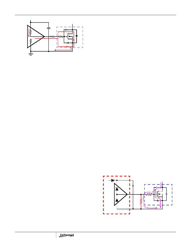
�Upper� MOSFET� Self� Turn-on� Effects� at� Start-up�
�S�
�FIGURE� 4.� TYPICAL� LOWER-GATE� DRIVE� TURN-ON� PATH�
�Application� Information�
�MOSFET� and� Driver� Selection�
�The� parasitic� inductances� of� the� PCB� and� of� the� power�
�devices’� packaging� (both� upper� and� lower� MOSFETs)� can�
�cause� serious� ringing,� exceeding� the� device’s� absolute�
�maximum� ratings.� The� negative� ringing� at� the� edges� of� the�
�PHASE� node� could� increase� the� bootstrap� capacitor� voltage�
�through� the� internal� bootstrap� diode,� and� in� some� cases,� it�
�may� overstress� the� upper� MOSFET� driver.� Careful� layout,�
�proper� selection� of� MOSFETs� and� packaging,� as� well� as� the�
�driver� can� minimize� such� unwanted� stress.�
�The� selection� of� D� 2� -PAK,� or� D-PAK� packaged� MOSFETs,� is�
�a� much� better� match� (for� the� reasons� discussed)� for� the�
�ISL6620A.� Low-profile� MOSFETs,� such� as� Direct� FETs� and�
�multi-source� leads� devices� (SO-8,� LFPAK,� PowerPAK),� have�
�low� parasitic� lead� inductances� and� can� be� driven� by� either�
�ISL6620� or� ISL6620A� (assuming� proper� layout� design).� The�
�ISL6620,� missing� the� 3� Ω� integrated� BOOT� resistor,� typically�
�yields� slightly� higher� efficiency� than� the� ISL6620A.�
�Should� the� driver� have� insufficient� bias� voltage� applied,� its�
�outputs� are� floating.� If� the� input� bus� is� energized� at� a� high�
�dV/dt� rate� while� the� driver� outputs� are� floating,� due� to� self�
�coupling� via� the� internal� C� GD� of� the� MOSFET,� the� gate� of� the�
�upper� MOSFET� could� momentarily� rise� up� to� a� level� greater�
�than� the� threshold� voltage� of� the� device,� potentially� turning�
�on� the� upper� switch.� Therefore,� if� such� a� situation� could�
�conceivably� be� encountered,� it� is� a� common� practice� to�
�place� a� resistor� (R� UGPH� )� across� the� gate� and� source� of� the�
�upper� MOSFET� to� suppress� the� Miller� coupling� effect.� The�
�value� of� the� resistor� depends� mainly� on� the� input� voltage’s�
�rate� of� rise,� the� C� GD� /C� GS� ratio,� as� well� as� the� gate-source�
�threshold� of� the� upper� MOSFET.� A� higher� dV/dt,� a� lower�
�C� DS� /C� GS� ratio,� and� a� lower� gate-source� threshold� upper�
�FET� will� require� a� smaller� resistor� to� diminish� the� effect� of�
�the� internal� capacitive� coupling.� For� most� applications,� the�
�integrated� 20k� Ω� resistor� is� sufficient,� not� affecting� normal�
�performance� and� efficiency.�
�The� coupling� effect� can� be� roughly� estimated� using� Equation� 5,�
�which� assumes� a� fixed� linear� input� ramp� and� neglects� the�
�clamping� effect� of� the� body� diode� of� the� upper� drive� and� the�
�bootstrap� capacitor.� Other� parasitic� components,� such� as� lead�
�inductances� and� PCB� capacitances,� are� also� not� taken� into�
�account.� Figure� 5� provides� a� visual� reference� for� this�
�phenomenon� and� its� potential� solution.�
�–� V�
�?�
�----------------------------------� ?�
�?� dV� ?�
�V� GS_MILLER� =� -------� ?� R� ?� C� rss� ?� 1� –� e� dt�
�iss� ?�
�------� ?� R� ?� C�
�Layout� Considerations�
�FA� good� layout� helps� reduce� the� ringing� on� the� switching�
�node� (PHASE)� and� significantly� lower� the� stress� applied� to�
�the� output� drives.� The� following� advice� is� meant� to� lead� to� an�
�dV�
�DS�
�dt� ?� ?�
�?� ?�
�?� ?�
�(EQ.� 5)�
�optimized� layout:�
�?� Keep� decoupling� loops� (VCC-GND� and� BOOT-PHASE)� as�
�R� =� R� UGPH� +� R� GI�
�C� rss� =� C� GD�
�C� iss� =� C� GD� +� C� GS�
�short� as� possible.�
�?� Minimize� trace� inductance,� especially� on� low-impedance�
�lines.� All� power� traces� (UGATE,� PHASE,� LGATE,� GND,�
�VCC)� should� be� short� and� wide,� as� much� as� possible.�
�?� Minimize� the� inductance� of� the� PHASE� node.� Ideally,� the�
�UVCC�
�BOOT�
�C� BOOT�
�C� GD�
�VIN�
�D�
�source� of� the� upper� and� the� drain� of� the� lower� MOSFET�
�should� be� as� close� as� thermally� allowable.�
�?� Minimize� the� current� loop� of� the� output� and� input� power�
�DU�
�DL�
�UGATE�
�G�
�R� GI�
�C� DS�
�trains.� Short� the� source� connection� of� the� lower� MOSFET�
�to� ground� as� close� to� the� transistor� pin� as� feasible.� Input�
�capacitors� (especially� ceramic� decoupling)� should� be�
�PHASE�
�C� GS�
�S�
�Q� UPPER�
�placed� as� close� to� the� drain� of� upper� and� source� of� lower�
�MOSFETs� as� possible.�
�FIGURE� 5.� GATE� TO� SOURCE� RESISTOR� TO� REDUCE�
�UPPER� MOSFET� MILLER� COUPLING�
�8�
�FN6494.0�
�April� 25,� 2008�
�相关PDF资料 |
PDF描述 |
|---|---|
| NMN0.75BK75 | NYLON MULTI 3/4" BLACK 75' |
| MBR2535CTG | DIODE SCHOTTKY 35V 30A TO220AB |
| T95Z336K016CSSL | CAP TANT 33UF 16V 10% 2910 |
| ABM43DRMH | CONN EDGECARD 86POS .156 WW |
| EEM18DRMT-S288 | CONN EDGECARD 36POS .156 EXTEND |
相关代理商/技术参数 |
参数描述 |
|---|---|
| ISL6620IRZ-T | 功能描述:IC MOSFET DVR SYNC BUCK 10-DFN RoHS:是 类别:集成电路 (IC) >> PMIC - MOSFET,电桥驱动器 - 外部开关 系列:- 标准包装:6,000 系列:* |
| ISL6622ACBZ | 功能描述:IC MOSFET DRVR SYNC BUCK 8-SOIC RoHS:是 类别:集成电路 (IC) >> PMIC - MOSFET,电桥驱动器 - 外部开关 系列:- 标准包装:50 系列:- 配置:高端 输入类型:非反相 延迟时间:200ns 电流 - 峰:250mA 配置数:1 输出数:1 高端电压 - 最大(自引导启动):600V 电源电压:12 V ~ 20 V 工作温度:-40°C ~ 125°C 安装类型:通孔 封装/外壳:8-DIP(0.300",7.62mm) 供应商设备封装:8-DIP 包装:管件 其它名称:*IR2127 |
| ISL6622ACBZ-T | 功能描述:IC MOSFET DRVR SYNC BUCK 8-SOIC RoHS:是 类别:集成电路 (IC) >> PMIC - MOSFET,电桥驱动器 - 外部开关 系列:- 标准包装:50 系列:- 配置:高端 输入类型:非反相 延迟时间:200ns 电流 - 峰:250mA 配置数:1 输出数:1 高端电压 - 最大(自引导启动):600V 电源电压:12 V ~ 20 V 工作温度:-40°C ~ 125°C 安装类型:通孔 封装/外壳:8-DIP(0.300",7.62mm) 供应商设备封装:8-DIP 包装:管件 其它名称:*IR2127 |
| ISL6622ACRZ | 功能描述:IC MOSFET DRVR SYNC BUCK 10-DFN RoHS:是 类别:集成电路 (IC) >> PMIC - MOSFET,电桥驱动器 - 外部开关 系列:- 标准包装:50 系列:- 配置:高端 输入类型:非反相 延迟时间:200ns 电流 - 峰:250mA 配置数:1 输出数:1 高端电压 - 最大(自引导启动):600V 电源电压:12 V ~ 20 V 工作温度:-40°C ~ 125°C 安装类型:通孔 封装/外壳:8-DIP(0.300",7.62mm) 供应商设备封装:8-DIP 包装:管件 其它名称:*IR2127 |
| ISL6622ACRZ-T | 功能描述:IC MOSFET DRVR SYNC BUCK 10-DFN RoHS:是 类别:集成电路 (IC) >> PMIC - MOSFET,电桥驱动器 - 外部开关 系列:- 标准包装:50 系列:- 配置:高端 输入类型:非反相 延迟时间:200ns 电流 - 峰:250mA 配置数:1 输出数:1 高端电压 - 最大(自引导启动):600V 电源电压:12 V ~ 20 V 工作温度:-40°C ~ 125°C 安装类型:通孔 封装/外壳:8-DIP(0.300",7.62mm) 供应商设备封装:8-DIP 包装:管件 其它名称:*IR2127 |
发布紧急采购,3分钟左右您将得到回复。