参数资料
| 型号: | ISL6752AAZA-T |
| 厂商: | Intersil |
| 文件页数: | 14/16页 |
| 文件大小: | 0K |
| 描述: | IC REG CTRLR PWM CM 16-QSOP |
| 标准包装: | 2,500 |
| PWM 型: | 电流模式 |
| 输出数: | 6 |
| 频率 - 最大: | 2MHz |
| 占空比: | 100% |
| 电源电压: | 9 V ~ 16 V |
| 降压: | 无 |
| 升压: | 无 |
| 回扫: | 无 |
| 反相: | 无 |
| 倍增器: | 无 |
| 除法器: | 无 |
| Cuk: | 无 |
| 隔离: | 无 |
| 工作温度: | -40°C ~ 105°C |
| 封装/外壳: | 16-SSOP(0.154",3.90mm 宽) |
| 包装: | 带卷 (TR) |
�� �
�
�ISL6752�
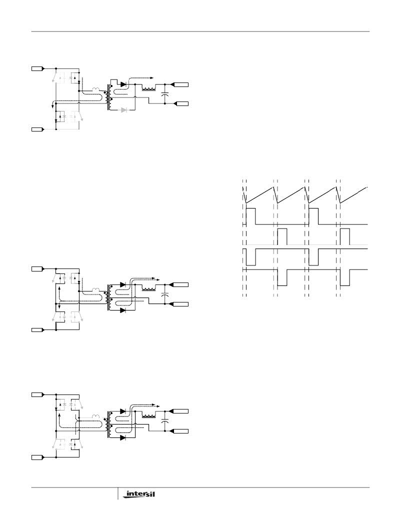
�The� second� power� transfer� period� commences� when� switch�
�LL� closes.� With� switches� UR� and� LL� on,� the� primary� and�
�secondary� currents� flow,� as� indicated� in� Figure� 13.�
�The� first� power� transfer� period� commences� when� switch� LR�
�closes� and� the� cycle� repeats.� The� ZVS� transition� requires�
�that� the� leakage� inductance� has� sufficient� energy� stored� to�
�VIN+�
�UL�
�UR�
�L� L�
�D1�
�VOUT+�
�fully� charge� the� parasitic� capacitances.� Since� the� energy�
�stored� is� proportional� to� the� square� of� the� current� (1/2� L� L� I� P2� ),�
�the� ZVS� resonant� transition� is� load� dependent.� If� the� leakage�
�inductance� is� not� able� to� store� sufficient� energy� for� ZVS,� a�
�discrete� inductor� may� be� added� in� series� with� the�
�RTN�
�transformer� primary.�
�LL�
�LR�
�D2�
�Synchronous� Rectifier� Outputs� and� Control�
�VIN-�
�FIGURE� 13.� UR� -� LL� POWER� TRANSFER� CYCLE�
�The� UR� -� LL� power� transfer� period� terminates� when� switch�
�LL� turns� off,� as� determined� by� the� PWM.� The� current� flowing�
�in� the� primary� must� find� an� alternate� path.� The� current� flows�
�into� the� parasitic� switch� capacitance,� which� charges� the�
�node� to� VIN� and� then� forward� biases� the� body� diode� of�
�upper� switch� UL.� As� before,� the� output� inductor� current�
�assists� in� this� transition.� The� primary� leakage� inductance,�
�L� L� ,� maintains� the� current,� which� now� circulates� around� the�
�path� of� switch� UR,� the� transformer� primary,� and� switch� UL.�
�When� switch� LL� opens,� the� output� inductor� current� free�
�wheels� predominantly� through� diode� D1.� Diode� D2� may�
�actually� conduct� very� little� or� none� of� the� free-wheeling�
�current,� depending� on� circuit� parasitics.� This� condition�
�persists� through� the� remainder� of� the� half-cycle.�
�The� ISL6752� provides� double-ended� PWM� outputs,� OUTLL�
�and� OUTLR,� and� synchronous� rectifier� (SR)� outputs,�
�OUTLLN� and� OUTLRN.� The� SR� outputs� are� the�
�complements� of� the� PWM� outputs.� It� should� be� noted� that�
�the� complemented� outputs� are� used� in� conjunction� with� the�
�opposite� PWM� output,� i.e.� OUTLL� and� OUTLRN� are� paired�
�together� and� OUTLR� and� OUTLLN� are� paired� together.�
�CT�
�OUTLL�
�OUTLR�
�OUTLLN�
�(SR1)�
�VIN+�
�UL�
�UR�
�L� L�
�D1�
�I� S�
�VOUT+�
�OUTLRN�
�(SR2)�
�I� P�
�RTN�
�FIGURE� 16.� BASIC� WAVEFORM� TIMING�
�LL�
�LR�
�D2�
�Referring� to� Figure� 16,� the� SRs� alternate� between� being� both�
�on� during� the� free-wheeling� portion� of� the� cycle� (OUTLL/LR�
�VIN-�
�FIGURE� 14.� UR� -� UL� FREE-WHEELING� PERIOD�
�When� the� upper� switches� toggle,� the� primary� current� that� was�
�flowing� through� UR� must� find� an� alternate� path.� It�
�charges/discharges� the� parasitic� capacitance� of� switches� UR�
�and� LR� until� the� body� diode� of� LR� is� forward-biased.� If� RESDEL�
�is� set� properly,� switch� LR� will� be� turned� on� at� this� time.�
�off),� and� one� or� the� other� being� off� when� OUTLL� or� OUTLR� is�
�on.� If� OUTLL� is� on,� its� corresponding� SR� must� also� be� on,�
�indicating� that� OUTLRN� is� the� correct� SR� control� signal.�
�Likewise,� if� OUTLR� is� on,� its� corresponding� SR� must� also� be�
�on,� indicating� that� OUTLLN� is� the� correct� SR� control� signal.�
�A� useful� feature� of� the� ISL6752� is� the� ability� to� vary� the�
�phase� relationship� between� the� PWM� outputs� (OUTLL,� OUT�
�VIN+�
�UL�
�UR�
�L� L�
�D1�
�I� S�
�VOUT+�
�LR)� and� their� complements� (OUTLLN,� OUTLRN)� by� ±300ns.�
�This� feature� allows� the� designer� to� compensate� for�
�differences� in� the� propagation� times� between� the� PWM� FETs�
�and� the� SR� FETs.� A� voltage� applied� to� VADJ� controls� the�
�LL�
�I� P�
�LR�
�RTN�
�phase� relationship.�
�D2�
�VIN-�
�FIGURE� 15.� UPPER� SWITCH� TOGGLE� AND� RESONANT�
�TRANSITION�
�14�
�FN9181.3�
�October� 31,� 2008�
�相关PDF资料 |
PDF描述 |
|---|---|
| ISL6753AAZA | IC REG CTRLR PWM CM/VM 16-QSOP |
| ISL6754AAZA | IC REG CTRLR PWM CM/VM 20-QSOP |
| ISL6755AAZA | IC REG CTRLR PWM CM/VM 20-QSOP |
| ISL6845IU-T | IC REG CTRLR BST FLYBK ISO 8MSOP |
| ISL6884IAZ | IC CTRLR CCFL BRIGHTNESS 20-SSOP |
相关代理商/技术参数 |
参数描述 |
|---|---|
| ISL6752AAZA-TR5325 | 制造商:Intersil Corporation 功能描述:ZVS Full-Bridge Current-Mode PWM with Adjustable Synchronous Rectifier Control |
| ISL6752DBEVAL1Z | 功能描述:BOARD DEMO FOR ISL6752 RoHS:是 类别:编程器,开发系统 >> 评估板 - DC/DC 与 AC/DC(离线)SMPS 系列:* 标准包装:1 系列:- 主要目的:DC/DC,步降 输出及类型:1,非隔离 功率 - 输出:- 输出电压:3.3V 电流 - 输出:3A 输入电压:4.5 V ~ 28 V 稳压器拓扑结构:降压 频率 - 开关:250kHz 板类型:完全填充 已供物品:板 已用 IC / 零件:L7981 其它名称:497-12113STEVAL-ISA094V1-ND |
| ISL6752EVAL1Z | 功能描述:EVALUATION BOARD FOR ISL6752 RoHS:是 类别:编程器,开发系统 >> 过时/停产零件编号 系列:- 标准包装:1 系列:- 传感器类型:CMOS 成像,彩色(RGB) 传感范围:WVGA 接口:I²C 灵敏度:60 fps 电源电压:5.7 V ~ 6.3 V 嵌入式:否 已供物品:成像器板 已用 IC / 零件:KAC-00401 相关产品:4H2099-ND - SENSOR IMAGE WVGA COLOR 48-PQFP4H2094-ND - SENSOR IMAGE WVGA MONO 48-PQFP |
| ISL6753AAZA | 功能描述:IC REG CTRLR PWM CM/VM 16-QSOP RoHS:是 类别:集成电路 (IC) >> PMIC - 稳压器 - DC DC 切换控制器 系列:- 产品培训模块:Lead (SnPb) Finish for COTS Obsolescence Mitigation Program 标准包装:2,500 系列:- PWM 型:电流模式 输出数:1 频率 - 最大:275kHz 占空比:50% 电源电压:18 V ~ 110 V 降压:无 升压:无 回扫:无 反相:无 倍增器:无 除法器:无 Cuk:无 隔离:是 工作温度:-40°C ~ 85°C 封装/外壳:8-SOIC(0.154",3.90mm 宽) 包装:带卷 (TR) |
| ISL6753AAZA-T | 功能描述:IC REG CTRLR PWM CM/VM 16-QSOP RoHS:是 类别:集成电路 (IC) >> PMIC - 稳压器 - DC DC 切换控制器 系列:- 产品培训模块:Lead (SnPb) Finish for COTS Obsolescence Mitigation Program 标准包装:2,500 系列:- PWM 型:电流模式 输出数:1 频率 - 最大:275kHz 占空比:50% 电源电压:18 V ~ 110 V 降压:无 升压:无 回扫:无 反相:无 倍增器:无 除法器:无 Cuk:无 隔离:是 工作温度:-40°C ~ 85°C 封装/外壳:8-SOIC(0.154",3.90mm 宽) 包装:带卷 (TR) |
发布紧急采购,3分钟左右您将得到回复。