- 您现在的位置:买卖IC网 > PDF目录17331 > ISL8107EVAL2Z (Intersil)EVAL BOARD 2 FOR ISL8107 PDF资料下载
参数资料
| 型号: | ISL8107EVAL2Z |
| 厂商: | Intersil |
| 文件页数: | 14/16页 |
| 文件大小: | 0K |
| 描述: | EVAL BOARD 2 FOR ISL8107 |
| 标准包装: | 1 |
| 系列: | * |
�� �
�
�ISL8107�
�6.� Calculate� R� 1� such� that� the� placement� of� F� Z2� is� at� the� F� LC� .�
�R� 1� =� --------------------------------------� –� R� 3�
�1�
�2� π� ×� C� 3� ×� F� LC�
�(EQ.� 18)�
�F� Z1� F� Z2�
�F� P1�
�MODULATOR� GAIN�
�COMPENSATION� GAIN�
�LOOP� GAIN�
�OPEN� LOOP� E/A� GAIN�
�R� 4� =� -------------------------------------� � R� 1�
�7.� Calculate� R� 4� based� on� target� output� voltage.�
�V� REF�
�V� OUT� –� V� REF�
�(EQ.� 19)�
�F� P2�
�20� log� ?� --------� ?�
�MAX� ?� V� IN�
�OSC�
�It� is� recommended� that� a� mathematical� model� be� used� to�
�plot� the� loop� response.� Check� the� loop� gain� against� the� error�
�amplifier� ’s� open-loop� gain.� Verify� phase� margin� results� and�
�adjust� as� necessary.� Equations� 20� and� 21� describe� the�
�0�
�R2�
�?� R1� ?�
�D�
�20� log� ----------------------------------�
�V�
�G� CL�
�G� FB�
�frequency� response� of� the� buck� converter� in� continuous�
�conduction� mode� (G� vd� ),� feedback� compensation� (G� comp� )�
�and� loop� response� (G� LP� ):�
�LOG�
�F� LC�
�F� CE�
�F� 0�
�G� MOD�
�FREQUENCY�
�G� vd� (� f� )� =� -------------------------------� ?� -----------------------------------------------------------------------------------------------------------�
�V� OSC�
�1� +� s� (� f� )� ?� (� ESR� +� DCR� )� ?� C� +� s� (� f� )� ?� L� ?� C�
�D� MAX� ?� V� IN� 1� +� s� (� f� )� ?� ESR� ?� C�
�2�
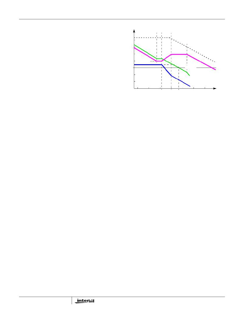
�FIGURE� 16.� ASYMPTOTIC� BODE� PLOT� OF� CONVERTER� GAIN�
�target� crossover� frequencies� in� the� range� of� 10%� to� 30%� of�
�1� +� s� (� f� )� ?� R� 2� ?� C� 1�
�s� (� f� )� ?� R� 1� ?� (� C� 1� +� C� 2� )�
�1� +� s� (� f� )� ?� (� R� 1� +� R� 3� )� ?� C� 3�
�(� 1� +� s� (� f� )� ?� R� 3� ?� C� 3� )� ?� ?� 1� +� s� (� f� )� ?� R� 2� ?� ---------------------� ?�
�G� COMP� (� f� )� =� ----------------------------------------------------� ?�
�--------------------------------------------------------------------------------------------------------------------�
�?� C� 1� ?� C� 2� ?�
�?� C� 1� +� C� 2� ?�
�(EQ.� 20)�
�the� switching� frequency� (F� SW� ).�
�Layout� Considerations�
�As� in� any� high� frequency� switching� converter,� layout� is� very�
�important.� Switching� current� from� one� power� device� to�
�another� can� generate� voltage� transients� across� the�
�impedances� of� the� interconnecting� bond� wires� and� circuit�
�G� LP� (� f� )� =� G� vd� (� f� )� ?� G� COMP� (� f� )�
�where� ,� s� (� f� )� =� 2� π� ?� f� ?� j�
�traces.� These� interconnecting� impedances� should� be�
�minimized� by� using� wide,� short� printed� circuit� traces.� The�
�COMPENSATION� BREAK� FREQUENCY� EQUATIONS�
�critical� components� should� be� located� as� close� together� as�
�possible� using� ground� plane� construction� or� single� point�
�F� Z1� =� -------------------------------�
�F� Z2� =� -------------------------------------------------�
�F� P1� =� -------------------------------�
�F� P2� =� ---------------------------------------------�
�2� π� ?� R� 2� ?� ---------------------�
�1�
�2� π� ?� R� 2� ?� C� 1�
�1�
�2� π� ?� (� R� 1� +� R� 3� )� ?� C� 3�
�1�
�2� π� ?� R� 3� ?� C� 3�
�1�
�C� 1� ?� C� 2�
�C� 1� +� C� 2�
�(EQ.� 21)�
�grounding.�
�A� multi-layer� printed� circuit� board� is� recommended.�
�Figure� 17� shows� the� critical� components� of� the� converter.�
�Note� that� capacitors� C� IN� and� C� OUT� could� each� represent�
�numerous� physical� capacitors.� Dedicate� one� solid� layer,�
�(usually� a� middle� layer� of� the� PC� board)� for� a� ground� plane�
�Figure� 16� shows� an� asymptotic� plot� of� the� DC/DC� converter’s�
�gain� vs� frequency.� The� actual� Modulator� Gain� has� a� high� gain�
�peak� dependent� on� the� quality� factor� (Q)� of� the� output� filter,�
�which� is� not� shown.� Using� the� previous� guidelines� should� yield�
�a� compensation� gain� similar� to� the� curve� plotted.� The� open� loop�
�error� amplifier� gain� bounds� the� compensation� gain.� Check� the�
�compensation� gain� at� F� P2� against� the� capabilities� of� the� error�
�amplifier.� The� loop� gain,� G� LP� ,� is� constructed� on� the� log-log�
�graph� of� Figure� 16� by� adding� the� modulator� gain,� G� vd� (in�
�dB),� to� the� feedback� compensation� gain,� G� COMP� (in� dB).�
�This� is� equivalent� to� multiplying� the� modulator� transfer�
�function� and� the� compensation� transfer� function� and� then�
�plotting� the� resulting� gain.�
�A� stable� control� loop� has� a� gain� crossing� with� close� to� a�
�-20dB/decade� slope� and� a� phase� margin� greater� than� 45°.�
�Include� worst� case� component� variations� when� determining�
�phase� margin.� The� mathematical� model� presented� makes� a�
�number� of� approximations� and� is� generally� not� accurate� at�
�frequencies� approaching� or� exceeding� half� the� switching�
�frequency.� When� designing� compensation� networks,� select�
�14�
�and� make� all� critical� component� ground� connections� with�
�vias� to� this� layer.� Dedicate� another� solid� layer� as� a� power�
�plane� and� break� this� plane� into� smaller� islands� of� common�
�voltage� levels.� Keep� the� metal� runs� from� the� PHASE�
�terminals� to� the� output� inductor� short.� The� power� plane�
�should� support� the� input� power� and� output� power� nodes.�
�Use� copper� filled� polygons� on� the� top� and� bottom� circuit�
�layers� for� the� PHASE� nodes.� Use� the� remaining� printed�
�circuit� layers� for� small� signal� wiring.�
�FN6605.0�
�October� 29,� 2008�
�相关PDF资料 |
PDF描述 |
|---|---|
| AS1PKHM3/85A | DIODE STD 1.5A 800V ESMP |
| AS1PJHM3/85A | DIODE STD 1.5A 600V ESMP |
| GMC10DRTN | CONN EDGECARD 20POS DIP .100 SLD |
| AS1PGHM3/85A | DIODE STD 1.5A 400V ESMP |
| AS1PDHM3/85A | DIODE STD 1.5A 200V ESMP |
相关代理商/技术参数 |
参数描述 |
|---|---|
| ISL8107IRZ | 功能描述:IC REG CTRLR BUCK PWM VM 16-QFN RoHS:是 类别:集成电路 (IC) >> PMIC - 稳压器 - DC DC 切换控制器 系列:- 产品培训模块:Lead (SnPb) Finish for COTS Obsolescence Mitigation Program 标准包装:2,500 系列:- PWM 型:电流模式 输出数:1 频率 - 最大:275kHz 占空比:50% 电源电压:18 V ~ 110 V 降压:无 升压:无 回扫:无 反相:无 倍增器:无 除法器:无 Cuk:无 隔离:是 工作温度:-40°C ~ 85°C 封装/外壳:8-SOIC(0.154",3.90mm 宽) 包装:带卷 (TR) |
| ISL8107IRZ-T | 功能描述:IC REG CTRLR BUCK PWM VM 16-QFN RoHS:是 类别:集成电路 (IC) >> PMIC - 稳压器 - DC DC 切换控制器 系列:- 产品培训模块:Lead (SnPb) Finish for COTS Obsolescence Mitigation Program 标准包装:2,500 系列:- PWM 型:电流模式 输出数:1 频率 - 最大:275kHz 占空比:50% 电源电压:18 V ~ 110 V 降压:无 升压:无 回扫:无 反相:无 倍增器:无 除法器:无 Cuk:无 隔离:是 工作温度:-40°C ~ 85°C 封装/外壳:8-SOIC(0.154",3.90mm 宽) 包装:带卷 (TR) |
| ISL8112 | 制造商:INTERSIL 制造商全称:Intersil Corporation 功能描述:High Light-Load Efficiency, Dual-Output, Main Power Supply Controllers |
| ISL8112EVAL1Z | 功能描述:EVALUATION BOARD FOR ISL8112 RoHS:是 类别:编程器,开发系统 >> 评估板 - DC/DC 与 AC/DC(离线)SMPS 系列:- 产品培训模块:Obsolescence Mitigation Program 标准包装:1 系列:True Shutdown™ 主要目的:DC/DC,步升 输出及类型:1,非隔离 功率 - 输出:- 输出电压:- 电流 - 输出:1A 输入电压:2.5 V ~ 5.5 V 稳压器拓扑结构:升压 频率 - 开关:3MHz 板类型:完全填充 已供物品:板 已用 IC / 零件:MAX8969 |
发布紧急采购,3分钟左右您将得到回复。