参数资料
| 型号: | ISL8107IRZ |
| 厂商: | Intersil |
| 文件页数: | 13/16页 |
| 文件大小: | 0K |
| 描述: | IC REG CTRLR BUCK PWM VM 16-QFN |
| 标准包装: | 60 |
| PWM 型: | 电压模式 |
| 输出数: | 1 |
| 频率 - 最大: | 600kHz |
| 电源电压: | 9 V ~ 75 V |
| 降压: | 是 |
| 升压: | 无 |
| 回扫: | 无 |
| 反相: | 无 |
| 倍增器: | 无 |
| 除法器: | 无 |
| Cuk: | 无 |
| 隔离: | 无 |
| 工作温度: | -40°C ~ 85°C |
| 封装/外壳: | 16-VQFN 裸露焊盘 |
| 包装: | 管件 |
�� �
�
�ISL8107�
�Rectifier� Selection�
�Power� Schottky� diode� is� recommended� for� better� converter�
�efficiency.� The� rectifier's� rated� reverse� breakdown� voltage�
�must� be� at� least� equal� to� the� maximum� input� voltage,�
�preferably� with� a� 20%� derating� factor.� The� power� dissipation�
�is� shown� in� Equation� 11:�
�break� frequency� at� F� LC� and� a� zero� at� F� CE� .� The� DC� gain� of�
�the� modulator� is� simply� the� input� voltage� (V� IN� )� divided� by� the�
�peak-to-peak� oscillator� voltage� Δ� V� OSC� .� The� ISL8107�
�incorporates� a� feed� forward� loop� that� accounts� for� changes�
�in� the� input� voltage.� This� maintains� a� constant� modulator�
�gain.�
�P� D� [� W� ]� =� I� OUT� ?� V� D� ?� ?� 1� –� ----------------� ?�
�?� V� OUT� ?�
�?� V� IN� ?�
�(EQ.� 11)�
�For� the� purpose� of� this� analysis,� L� and� DCR� represent� the�
�output� inductance� and� its� DCR,� while� C� and� ESR� represents�
�the� total� output� capacitance� and� its� equivalent� series�
�where� V� D� is� the� voltage� of� the� Schottky� diode� =� 0.5V� to� 0.7V�
�resistance� in� Equation� 12.�
�F� LC� =� ---------------------------�
�F� CE� =� ---------------------------------�
�Application� Guidelines�
�1�
�2� π� ?� L� ?� C�
�1�
�2� π� ?� C� ?� ESR�
�(EQ.� 12)�
�Feedback� Compensation�
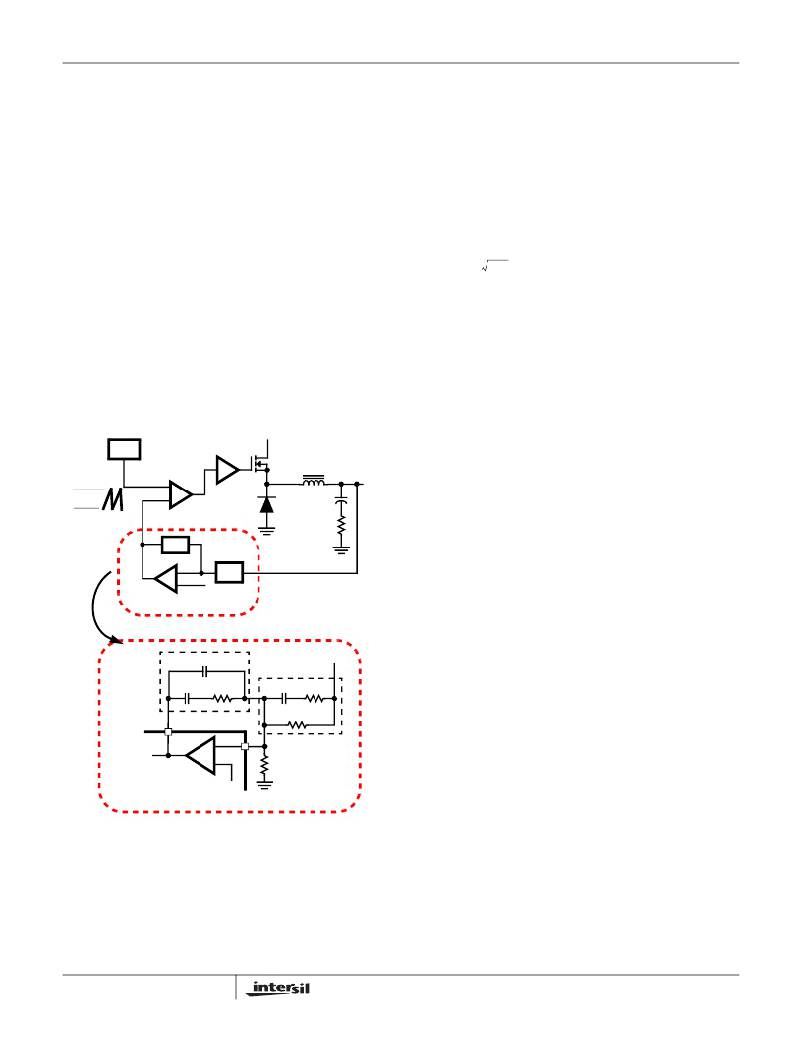
�Figure� 15� highlights� the� voltage-mode� control� loop� for� a� buck�
�converter� with� type-III� compensator.� The� output� voltage� is�
�regulated� to� the� reference� voltage� level.� The� error� amplifier�
�output� is� compared� with� the� oscillator� ramp� wave� to� provide�
�a� pulse-width� modulated� wave� with� an� amplitude� of� V� IN� at�
�the� PHASE� node.� The� PWM� wave� is� smoothed� by� the� output�
�filter.� The� output� filter� capacitor� bank’s� equivalent� series�
�resistance� is� represented� by� the� series� resistor� ESR.�
�The� compensation� network� consists� of� the� transconductance�
�amplifier� (internal� to� the� ISL8107)� and� the� external� R� 1� to� R� 4� ,�
�C� 1� to� C� 3� components.� The� goal� of� the� compensation� network�
�is� to� provide� a� closed� loop� transfer� function� with� high� 0dB�
�crossing� frequency� (F� 0� ;� typically� 0.1� to� 0.3� of� F� SW� )� and�
�adequate� phase� margin� (better� than� 45°).� Phase� margin� is� the�
�difference� between� the� closed� loop� phase� at� F� 0dB� and� 180°.�
�The� equations� that� follow� relate� the� compensation� network’s�
�poles,� zeros� and� gain� to� the� components� (R� 1� ,� R� 2� ,� R� 3� ,� R� 4� ,� C� 1� ,�
�-�
�-�
�C� 1� =� -------------------------------------�
�Δ� V� OSC�
�OSC�
�PWM�
�COMPARATOR�
�+�
�Z� FB�
�V� E/A�
�+�
�DRIVER�
�DRIVER�
�Z� IN�
�V� IN�
�L� O�
�LX�
�C� O�
�D�
�ESR�
�(PARASITIC)�
�V� OUT�
�C� 2� ,� and� C� 3� )� in� Figures� 4� and� 5.� Use� the� following� guidelines�
�for� locating� the� poles� and� zeros� of� the� compensation� network:�
�1.� Select� a� value� for� R� 2� ,� (10k� to� 100k� typically)�
�2.� Calculate� C� 1� such� that� F� Z1� is� placed� at� a� fraction� of� the� F� LC� ,�
�at� 0.1� to� 0.75� of� F� LC� .� The� higher� the� quality� factor� of� the�
�output� filter� and/or� the� higher� the� ratio� F� CE� /F� LC� ,� the� lower�
�the� F� Z1� frequency� (to� maximize� phase� boost� at� F� LC� ).�
�1�
�(EQ.� 13)�
�2� π� ×� F� Z1� ×� R� 2�
�ERROR�
�AMP�
�REFERENCE�
�3.� Calculate� C� 3� such� that� F� BW� is� placed� at� desired� frequency�
�(typically,� 0.1x� to� 0.5x� F� SW� ).� F� SW� represents� the�
�DETAILED� COMPENSATION� COMPONENTS�
�switching� frequency� of� the� regulator.�
�V� IN� � R� 2�
�C� 2�
�Z� FB�
�Z� IN�
�V� OUT�
�2� π� ×� F� BW� ×� L� ×� C� 0� ×� V� OSC�
�C� 3� =� ------------------------------------------------------------------------�
�(EQ.� 14)�
�C� 1�
�R� 2�
�C� 3�
�R� 3�
�ISL8107� has� feed� forward� compensation� that� adjusts� the�
�amplitude� of� 0.11*V� IN� .� Therefore,� the� Equation� 14� can� be�
�C� 3� =� ---------------------------------------------------------�
�COMP�
�g� m� -�
�+�
�FB�
�R� 4�
�R� 1�
�simplified� as� Equation� 15:�
�0.22� π� ×� F� BW� ×� L� ×� C� 0�
�R� 2�
�(EQ.� 15)�
�ISL8107�
�V� REF�
�4.� Calculate� C� 2� such� that� the� placement� of� F� P2� is� at� a� fraction�
�of� the� F� SW� .� The� lowering� of� the� frequency� helps� reduce�
�the� gain� of� the� compensation� network� at� high� frequency,�
�V� OUT� =� V� REF� � ?� 1� +� ------� 1� -� ?�
�C� 2� =� -------------------------------------�
�2� π� ×� F� P2� ×� R� 2�
�?� R� ?�
�?� R� 4� ?�
�FIGURE� 15.� VOLTAGE-MODE� BUCK� CONVERTER�
�COMPENSATION� DESIGN� AND� OUTPUT�
�VOLTAGE� SELECTION�
�in� turn� reducing� the� HF� ripple� component� at� the� COMP�
�pin� and� minimizing� resultant� duty� cycle� jitter.�
�1�
�(EQ.� 16)�
�5.� Calculate� R� 3� such� that� the� placement� of� F� P1� is� at� the� F� CE� .�
�R� 3� =� --------------------------------------�
�The� modulator� transfer� function� is� the� small-signal� transfer�
�function� of� V� OUT� /V� COMP� .� This� function� is� dominated� by� a�
�DC� gain� and� shaped� by� the� output� filter,� with� a� double� pole�
�13�
�1�
�2� π� ×� C� 3� ×� F� CE�
�(EQ.� 17)�
�FN6605.0�
�October� 29,� 2008�
�相关PDF资料 |
PDF描述 |
|---|---|
| ISL8118IRZ-T | IC REG CTRLR BUCK PWM VM 28-QFN |
| ISL8120IRZEC | IC REG CTRLR BUCK PWM VM 32-QFN |
| ISL8120IRZ | IC REG CTRLR BUCK PWM VM 32-QFN |
| ISL8121IRZ | IC REG CTRLR BUCK PWM VM 24-QFN |
| ISL8126IRZ | IC REG CTRLR BUCK PWM VM 32-QFN |
相关代理商/技术参数 |
参数描述 |
|---|---|
| ISL8107IRZ-T | 功能描述:IC REG CTRLR BUCK PWM VM 16-QFN RoHS:是 类别:集成电路 (IC) >> PMIC - 稳压器 - DC DC 切换控制器 系列:- 产品培训模块:Lead (SnPb) Finish for COTS Obsolescence Mitigation Program 标准包装:2,500 系列:- PWM 型:电流模式 输出数:1 频率 - 最大:275kHz 占空比:50% 电源电压:18 V ~ 110 V 降压:无 升压:无 回扫:无 反相:无 倍增器:无 除法器:无 Cuk:无 隔离:是 工作温度:-40°C ~ 85°C 封装/外壳:8-SOIC(0.154",3.90mm 宽) 包装:带卷 (TR) |
| ISL8112 | 制造商:INTERSIL 制造商全称:Intersil Corporation 功能描述:High Light-Load Efficiency, Dual-Output, Main Power Supply Controllers |
| ISL8112EVAL1Z | 功能描述:EVALUATION BOARD FOR ISL8112 RoHS:是 类别:编程器,开发系统 >> 评估板 - DC/DC 与 AC/DC(离线)SMPS 系列:- 产品培训模块:Obsolescence Mitigation Program 标准包装:1 系列:True Shutdown™ 主要目的:DC/DC,步升 输出及类型:1,非隔离 功率 - 输出:- 输出电压:- 电流 - 输出:1A 输入电压:2.5 V ~ 5.5 V 稳压器拓扑结构:升压 频率 - 开关:3MHz 板类型:完全填充 已供物品:板 已用 IC / 零件:MAX8969 |
| ISL8112IRZ | 功能描述:IC REG DL BCK/LINEAR SYNC 32-QFN RoHS:是 类别:集成电路 (IC) >> PMIC - 稳压器 - 线性 + 切换式 系列:- 标准包装:2,500 系列:- 拓扑:降压(降压)同步(3),线性(LDO)(2) 功能:任何功能 输出数:5 频率 - 开关:300kHz 电压/电流 - 输出 1:控制器 电压/电流 - 输出 2:控制器 电压/电流 - 输出 3:控制器 带 LED 驱动器:无 带监控器:无 带序列发生器:是 电源电压:5.6 V ~ 24 V 工作温度:-40°C ~ 85°C 安装类型:* 封装/外壳:* 供应商设备封装:* 包装:* |
发布紧急采购,3分钟左右您将得到回复。