参数资料
| 型号: | ISL9443IRZ-T7A |
| 厂商: | Intersil |
| 文件页数: | 19/23页 |
| 文件大小: | 0K |
| 描述: | IC REG CTRLR BUCK PWM CM 32-QFN |
| 标准包装: | 1 |
| PWM 型: | 电流模式 |
| 输出数: | 3 |
| 频率 - 最大: | 1.32MHz |
| 电源电压: | 4.5 V ~ 26 V |
| 降压: | 是 |
| 升压: | 无 |
| 回扫: | 无 |
| 反相: | 无 |
| 倍增器: | 无 |
| 除法器: | 无 |
| Cuk: | 无 |
| 隔离: | 无 |
| 工作温度: | -40°C ~ 85°C |
| 封装/外壳: | 32-VFQFN 裸露焊盘 |
| 包装: | 标准包装 |
| 其它名称: | ISL9443IRZ-T7ADKR |
�� �
�
�ISL9443�
�C2�
�Layout� Considerations�
�R2�
�C1�
�1.� The� input� capacitors,� upper� FET,� lower� FET,� inductor� and�
�CONVERTER�
�EA�
�G� M� =� 17.5dB�
�MODULATOR�
�R1�
�TYPE� 2� EA�
�G� EA� =� 18dB�
�output� capacitor� should� be� placed� first.� Isolate� these� power�
�components� on� the� topside� of� the� board� with� their� ground�
�terminals� adjacent� to� one� another.� Place� the� input� high�
�frequency� decoupling� ceramic� capacitors� very� close� to� the�
�MOSFETs.�
�2.� Use� separate� ground� planes� for� power� ground� and� small�
�signal� ground.� Connect� the� SGND� and� PGND� together� close� to�
�F� PO�
�F� Z�
�F� C�
�F� P�
�the� IC.� Do� not� connect� them� together� anywhere� else.�
�3.� The� loop� formed� by� the� input� capacitor,� the� top� FET� and� the�
�bottom� FET� must� be� kept� as� small� as� possible.�
�4.� Ensure� the� current� paths� from� the� input� capacitor� to� the�
�MOSFET,� to� the� output� inductor� and� output� capacitor� are� as�
�short� as� possible� with� maximum� allowable� trace� widths.�
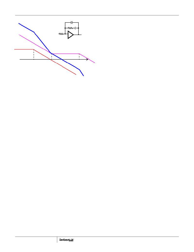
�FIGURE� 22.� FEEDBACK� LOOP� COMPENSATION�
�Conditional� stability� may� occur� only� when� the� main� load� pole� is�
�positioned� too� much� to� the� left� side� on� the� frequency� axis� due� to�
�excessive� output� filter� capacitance.� In� this� case,� the� ESR� zero�
�placed� within� the� 1.2kHz� to� 30kHz� range� gives� some� additional�
�phase� ‘boost’.� Some� phase� boost� can� also� be� achieved� by�
�connecting� capacitor� C� Z� in� parallel� with� the� upper� resistor� R� 1� of�
�the� divider� that� sets� the� output� voltage� value.� Please� refer� to�
��Layout� Guidelines�
�Careful� attention� to� layout� requirements� is� necessary� for�
�successful� implementation� of� an� ISL9443� based� DC/DC�
�converter.� The� ISL9443s� switch� at� a� very� high� frequency� and�
�therefore� the� switching� times� are� very� short.� At� these� switching�
�frequencies,� even� the� shortest� trace� has� significant� impedance.�
�Also,� the� peak� gate� drive� current� rises� significantly� in� an�
�extremely� short� time.� Transition� speed� of� the� current� from� one�
�device� to� another� causes� voltage� spikes� across� the�
�interconnecting� impedances� and� parasitic� circuit� elements.�
�These� voltage� spikes� can� degrade� efficiency,� generate� EMI,�
�increase� device� overvoltage� stress� and� ringing.� Careful�
�component� selection� and� proper� PC� board� layout� minimizes� the�
�magnitude� of� these� voltage� spikes.�
�There� are� three� sets� of� critical� components� in� a� DC/DC� converter�
�using� the� ISL9443:� The� controller,� the� switching� power�
�components� and� the� small� signal� components.� The� switching�
�power� components� are� the� most� critical� from� a� layout� point� of�
�view� because� they� switch� a� large� amount� of� energy,� so� they� tend�
�to� generate� a� large� amount� of� noise.� The� critical� small� signal�
�components� are� those� connected� to� sensitive� nodes� or� those�
�supplying� critical� bias� currents.� A� multi-layer� printed� circuit� board�
�is� recommended.�
�19�
�5.� Place� The� PWM� controller� IC� close� to� the� lower� FET.� The� LGATE�
�connection� should� be� short� and� wide.� The� IC� can� be� best�
�placed� over� a� quiet� ground� area.� Avoid� switching� ground� loop�
�currents� in� this� area.�
�6.� Place� the� VCC_5V� bypass� capacitor� very� close� to� the� VCC_5V�
�pin� of� the� IC� and� connect� its� ground� to� the� PGND� plane.�
�7.� Place� the� gate� drive� components� -� optional� BOOT� diode� and�
�BOOT� capacitors� -� together� near� the� controller� IC.�
�8.� The� output� capacitors� should� be� placed� as� close� to� the� load� as�
�possible.� Use� short� wide� copper� regions� to� connect� output�
�capacitors� to� load� to� avoid� inductance� and� resistances.�
�9.� Use� copper� filled� polygons� or� wide� but� short� trace� to� connect�
�the� junction� of� the� upper� FET,� Lower� FET� and� output� inductor.�
�Also,� keep� the� PHASE� node� connection� to� the� IC� short.� Do� not�
�unnecessarily� oversize� the� copper� islands� for� PHASE� node.�
�Since� the� phase� nodes� are� subjected� to� very� high� dv/dt�
�voltages,� the� stray� capacitor� formed� between� these� islands�
�and� the� surrounding� circuitry� will� tend� to� couple� switching�
�noise.�
�10.� Route� all� high� speed� switching� nodes� away� from� the� control�
�circuitry.�
�11.� Create� a� separate� small� analog� ground� plane� near� the� IC.�
�Connect� the� SGND� pin� to� this� plane.� All� small� signal� grounding�
�paths� including� feedback� resistors,� current� limit� setting�
�resistors,� soft-starting� capacitors� and� ENx� pull-down� resistors�
�should� be� connected� to� this� SGND� plane.�
�12.� Separate� current� sensing� traces� from� PHASE� node�
�connections.�
�13.� Ensure� the� feedback� connection� to� the� output� capacitor� is�
�short� and� direct.�
�FN7663.1�
�February� 24,� 2012�
�相关PDF资料 |
PDF描述 |
|---|---|
| ISL9444IRZ | IC REG CTRLR BUCK PWM CM 40-QFN |
| ISL9491ERZ | IC REG SGL LNB CONTROL 16QFN |
| ISL9492ERZ-T | IC REG SGL LNB CONTROL 28TQFN |
| ISL9506HRZ | IC REG CTRLR BUCK PWM 40-QFN |
| ISL95210IRZ | IC REG BUCK SYNC ADJ 10A 32QFN |
相关代理商/技术参数 |
参数描述 |
|---|---|
| ISL9443IRZ-T7AS2750 | 制造商:Intersil Corporation 功能描述:ISL9443 TRIPLE, STEP- DOWN PWM CONTROLLER IMVP-6. 32 LD MLFP - Tape and Reel |
| ISL9443IRZ-TS2750 | 制造商:Intersil Corporation 功能描述:PB FREE. ISL9443 TRIPLE, STEP- DOWN PWM CONTROLLER IMVP-6. 3 - Tape and Reel |
| ISL9444CRZ | 制造商:Intersil Corporation 功能描述:PB FREE. ISL9444 TRIPLE, STEP- DOWN PWM CONTROLLER IMVP-6. 4 - Rail/Tube 制造商:Intersil Corporation 功能描述:IC REG CTRLR BUCK PWM CM 32-QFN 制造商:Intersil 功能描述:Pb Free. ISL9444 Tri ple, Step- Down PWM |
| ISL9444CRZ-T | 制造商:Intersil Corporation 功能描述:PB FREE. ISL9444 TRIPLE, STEP- DOWN PWM CONTROLLER IMVP-6. 4 - Tape and Reel 制造商:Intersil Corporation 功能描述:IC REG CTRLR BUCK PWM CM 32-QFN 制造商:Intersil 功能描述:Pb Free. ISL9444 Tri ple, Step- Down PWM |
| ISL9444CRZ-T7A | 制造商:Intersil Corporation 功能描述:IC REG CTRLR BUCK PWM CM 32-QFN 制造商:INTERSIL 功能描述:ISL9444 Series 1.2 Mhz Triple Synchronous Step-Down PWM - QFN-40 制造商:Intersil 功能描述:ISL9444 Triple, Step - Down PWM Controlle 制造商:Intersil 功能描述:ISL9444 Series 1.2 Mhz Triple Synchronous Step-Down PWM - QFN-40 |
发布紧急采购,3分钟左右您将得到回复。