参数资料
| 型号: | ISL97652IRZ |
| 厂商: | Intersil |
| 文件页数: | 12/25页 |
| 文件大小: | 0K |
| 描述: | IC LCD SUPPLY HP 4CHN 48-QFN |
| 标准包装: | 43 |
| 应用: | LCD 电视机/监控器 |
| 电流 - 电源: | 500µA |
| 电源电压: | 8 V ~ 15 V |
| 工作温度: | -40°C ~ 85°C |
| 安装类型: | 表面贴装 |
| 封装/外壳: | 48-VFQFN 裸露焊盘 |
| 供应商设备封装: | 48-QFN(7x7) |
| 包装: | 管件 |
�� �
�
�ISL97652�
�The� boost� converter� uses� a� summing� amplifier� architecture�
�consisting� of� gm� stages� for� voltage� feedback,� current�
�feedback� and� slope� compensation.� A� comparator� looks� at�
�the� peak� inductor� current� cycle� by� cycle� and� terminates� the�
�PWM� cycle� if� the� current� limit� is� reached.�
�An� external� resistor� divider� is� required� to� divide� the� output�
�voltage� down� to� the� nominal� reference� voltage.� Current�
�drawn� by� the� resistor� network� should� be� limited� to� maintain�
�the� overall� converter� efficiency.� The� maximum� value� of� the�
�resistor� network� is� limited� by� the� feedback� input� bias� current�
�and� the� potential� for� noise� being� coupled� into� the� feedback�
�pin.� A� resistor� network� in� the� order� of� 60k� Ω� is� recommended.�
�The� boost� converter� output� voltage� is� determined� by� the�
�following� equation:�
�higher� frequency� option� is� selected.� The� minimum� boost�
�duty� cycle� of� the� ISL97652� is� ~10%� for� 650kHz� and� ~20%�
�for� 1.3MHz.� When� the� operating� duty� cycle� is� lower� than� the�
�minimum� duty� cycle,� the� part� will� not� switch� in� some� cycles�
�randomly,� which� will� cause� some� LX� pulses� to� be� skipped.� In�
�this� cas,� LX� pulses� are� not� consistent� any� more,� but� the�
�output� voltage� (A� VDD� )� is� still� regulated� by� the� ratio� of� R1� and�
�R2.� Because� some� LX� pulses� are� skipped,� the� ripple� current�
�in� the� inductor� will� become� bigger.� Under� the� worst� case,� the�
�ripple� current� will� be� from� 0� to� the� threshold� of� the� current�
�limit.� In� turn,� the� bigger� ripple� current� will� increase� the� output�
�voltage� ripple.� Hence,� it� will� need� more� output� capacitors� to�
�keep� the� output� ripple� at� the� same� level.� When� the� input�
�voltage� equals,� or� is� larger� than,� the� output� voltage,� the�
�boost� converter� will� stop� switching.� The� boost� converter� is�
�V� BOOST� =� ---------------------� � V� FB�
�R� 1� +� R� 2�
�R� 2�
�(EQ.� 2)�
�not� regulated� any� more,� but� the� part� will� still� be� on� and� other�
�channels� are� still� regulated.�
�I� OMAX� =� ?� I� LMT� –� --------� ?� ×� ---------�
�V� O�
�The� current� through� the� MOSFET� is� limited� to� 2.8Apeak.�
�This� restricts� the� maximum� output� current� (average)� based�
�on� the� following� equation:�
�Δ� I� L� V� IN� (EQ.� 3)�
�?� 2� ?�
�Where� Δ� IL� is� peak� to� peak� inductor� ripple� current,� and� is� set� by:�
�Boost� Converter� Input� Capacitor�
�An� input� capacitor� is� used� to� suppress� the� voltage� ripple�
�injected� into� the� boost� converter.� A� ceramic� capacitor� with�
�capacitance� larger� than� 10μF� is� recommended.� The� voltage�
�rating� of� input� capacitor� should� be� larger� than� the� maximum�
�input� voltage.� Some� capacitors� are� recommended� in� Table� 2�
�for� input� capacitor.�
�Δ� I� L� =� ---------� ×� -----�
�f� S�
�V� IN� D�
�L�
�(EQ.� 4)�
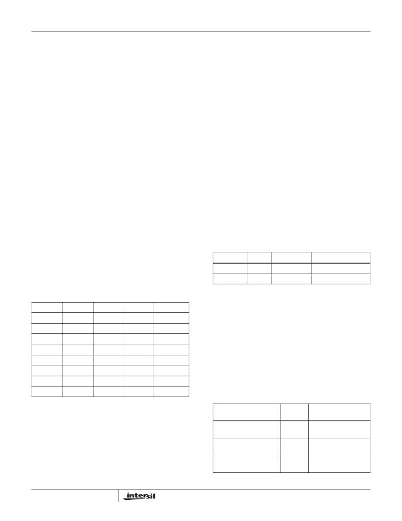
�TABLE� 2.� BOOST� CONVERTER� INPUT� CAPACITOR�
�RECOMMENDATION�
�where� f� s� is� the� switching� frequency�
�The� following� table� gives� typical� values� (margins� are�
�considered� 10%,� 3%,� 20%,� 10%� and� 15%� on� V� IN� ,� V� O� ,� L,� f� S�
�CAPACITOR�
�10μF/25V�
�10μF/25V�
�SIZE�
�1210�
�1210�
�VENDOR�
�TDK�
�Murata�
�PART� NUMBER�
�C3225X7R1E106M�
�GRM32DR61E106K�
�and� I� OMAX� ):�
�TABLE� 1.� MAXIMUM� OUTPUT� CURRENT� CALCULATION�
�Boost� Inductor�
�V� IN� (V)�
�12�
�12�
�12�
�V� O� (V)�
�15�
�15�
�18�
�L� (μH)�
�6.8�
�6.8�
�6.8�
�f� s� (MHz)�
�0.65�
�1.3�
�0.65�
�I� OMAX� (mA)�
�1890�
�1955�
�1500�
�The� boost� inductor� is� a� critical� part� which� influences� the�
�output� voltage� ripple,� transient� response,� and� efficiency.�
�Values� of� 3.3μH� to� 10μH� should� be� selected� to� match� the�
�internal� slope� compensation.� The� inductor� must� be� able� to�
�handle� the� following� average� and� peak� current:�
�I� LAVG� =� -------------�
�I� LPK� =� I� LAVG� +� --------�
�12�
�8�
�8�
�8�
�8�
�18�
�15�
�15�
�18�
�18�
�6.8�
�6.8�
�6.8�
�6.8�
�6.8�
�1.3�
�0.65�
�1.3�
�0.65�
�1.3�
�1590�
�1200�
�1275�
�950�
�1050�
�I� O�
�1� –� D�
�Δ� I� L�
�2�
�Some� inductors� are� recommended� in� Table� 3.�
�(EQ.� 5)�
�(EQ.� 6)�
�TABLE� 3.� BOOST� INDUCTOR� RECOMMENDATION�
�When� operating� at� the� lower� frequency� option,� 650kHz,� the�
�DIMENSIONS�
�potential� increase� in� ripple� current� in� the� inductor� can� be�
�INDUCTOR�
�(mm)� VENDOR�
�PART� NUMBER�
�avoided� by� increasing� the� inductor� by� the� same� factor.� This�
�6.8μH/�
�7.3x6.8x3.2�
�TDK�
�RLF7030T-6R8N3R0�
�allows� the� slope� compensation� in� the� boost� feedback� to�
�3A� PEAK�
�remain� the� same� as� the� 1.3MHz� case� and� this� will� maintain�
�stability� of� the� converter� over� the� widest� operating� range.�
�6.8μH/�
�2.9A� PEAK�
�7.6X7.6X3.0� Sumida�
�CDR7D28MNNP-6R8NC�
�Operation� at� 650kHz� allows� boost� operation� down� to� lower�
�minimum� duty� cycles,� where� the� output� voltage� required� is�
�closer� to� the� input� voltage� than� can� be� achieved� when� the�
�5.2μH/�
�4.55A� PEAK�
�10x10.1x3.8�
�Cooper�
�Bussmann�
�CD1-5R2�
�12�
�FN9287.1�
�November� 2,� 2007�
�相关PDF资料 |
PDF描述 |
|---|---|
| ISL97653AIRZ | IC LCD SUPPLY 5CHN 40-QFN |
| ISL97656IRTZ | IC REG BOOST ADJ 4A 10TDFN |
| ISL97701IRZ | IC REG BOOST ADJ 0.1A 10DFN |
| ISL97702IRZ-T7 | IC REG BOOST ADJ 0.13A DL 10DFN |
| ISL98012IUZ | IC REG BOOST ADJ 0.6A 10MSOP |
相关代理商/技术参数 |
参数描述 |
|---|---|
| ISL97652IRZ-T | 功能描述:IC LCD SUPPLY 4CH DUAL AMP 48QFN RoHS:是 类别:集成电路 (IC) >> PMIC - 电源管理 - 专用 系列:- 应用说明:Ultrasound Imaging Systems Application Note 产品培训模块:Lead (SnPb) Finish for COTS Obsolescence Mitigation Program 标准包装:37 系列:- 应用:医疗用超声波成像,声纳 电流 - 电源:- 电源电压:2.37 V ~ 6 V 工作温度:0°C ~ 70°C 安装类型:表面贴装 封装/外壳:56-WFQFN 裸露焊盘 供应商设备封装:56-TQFN-EP(8x8) 包装:管件 |
| ISL97652IRZ-TK | 功能描述:IC LCD SUPPLY 4CH DUAL AMP 48QFN RoHS:是 类别:集成电路 (IC) >> PMIC - 电源管理 - 专用 系列:- 应用说明:Ultrasound Imaging Systems Application Note 产品培训模块:Lead (SnPb) Finish for COTS Obsolescence Mitigation Program 标准包装:37 系列:- 应用:医疗用超声波成像,声纳 电流 - 电源:- 电源电压:2.37 V ~ 6 V 工作温度:0°C ~ 70°C 安装类型:表面贴装 封装/外壳:56-WFQFN 裸露焊盘 供应商设备封装:56-TQFN-EP(8x8) 包装:管件 |
| ISL97653AIRZ | 功能描述:电流型 PWM 控制器 5-CH INTEGRTD LCD SUPPLY W/TEMP SENSOR RoHS:否 制造商:Texas Instruments 开关频率:27 KHz 上升时间: 下降时间: 工作电源电压:6 V to 15 V 工作电源电流:1.5 mA 输出端数量:1 最大工作温度:+ 105 C 安装风格:SMD/SMT 封装 / 箱体:TSSOP-14 |
| ISL97653AIRZ-T | 功能描述:电流型 PWM 控制器 5-CH INTEGRTD LCD SUPPLY W/TEMP SENSOR RoHS:否 制造商:Texas Instruments 开关频率:27 KHz 上升时间: 下降时间: 工作电源电压:6 V to 15 V 工作电源电流:1.5 mA 输出端数量:1 最大工作温度:+ 105 C 安装风格:SMD/SMT 封装 / 箱体:TSSOP-14 |
| ISL97653AIRZ-TK | 功能描述:电流型 PWM 控制器 5-CH INTEGRTD LCD SUPPLY W/TEMP SENSOR RoHS:否 制造商:Texas Instruments 开关频率:27 KHz 上升时间: 下降时间: 工作电源电压:6 V to 15 V 工作电源电流:1.5 mA 输出端数量:1 最大工作温度:+ 105 C 安装风格:SMD/SMT 封装 / 箱体:TSSOP-14 |
发布紧急采购,3分钟左右您将得到回复。