- 您现在的位置:买卖IC网 > PDF目录19592 > ISPLSI 1048C-70LQ (Lattice Semiconductor Corporation)IC PLD ISP 96I/O 16NS 128PQFP PDF资料下载
参数资料
| 型号: | ISPLSI 1048C-70LQ |
| 厂商: | Lattice Semiconductor Corporation |
| 文件页数: | 9/15页 |
| 文件大小: | 0K |
| 描述: | IC PLD ISP 96I/O 16NS 128PQFP |
| 标准包装: | 24 |
| 系列: | ispLSI® 1000 |
| 可编程类型: | 系统内可编程 |
| 最大延迟时间 tpd(1): | 18.0ns |
| 电压电源 - 内部: | 4.75 V ~ 5.25 V |
| 逻辑元件/逻辑块数目: | 48 |
| 门数: | 8000 |
| 输入/输出数: | 96 |
| 工作温度: | 0°C ~ 70°C |
| 安装类型: | 表面贴装 |
| 封装/外壳: | 128-BQFP |
| 供应商设备封装: | 128-PQFP(28x28) |
| 包装: | 托盘 |
| 其它名称: | ISPLSI1048C-70LQ |
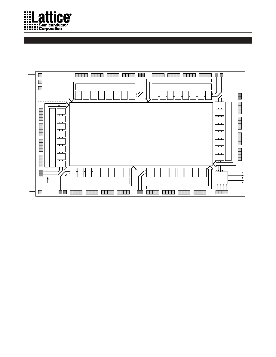
Specifications ispLSI 1048C
2
The device also has a 96 I/O cells, each of which is
directly connected to an I/O pin. Each I/O cell can be
individually programmed to be a combinatorial input,
registered input, latched input, output or bi-directional
I/O pin with 3-state control. Additionally, all outputs have
selectable polarity, active high or active low. The signal
voltage levels are TTL-compatible, and the output drivers
can source 4 mA or sink 8 mA.
Eight GLBs, 16 I/O cells, two dedicated inputs and one
ORP are connected together to make a Megablock as
shown in figure 1. The outputs of the eight GLBs are
connected to a set of 16 universal I/O cells by the ORP.
Each ispLSI 1048C device contains six Megablocks.
The GRP has, as its inputs, the outputs from all of the
GLBs and all of the inputs from the bi-directional I/O cells.
All of these signals are made available to the inputs of the
GLBs. Delays through the GRP have been equalized to
minimize timing skew.
Clocks in the ispLSI 1048C device are selected using the
Clock Distribution Network. Four dedicated clock pins
(Y0, Y1, Y2 and Y3) are brought into the distribution
network, and five clock outputs (CLK 0, CLK 1, CLK 2,
IOCLK 0 and IOCLK 1) are provided to route clocks to the
GLBs and I/O cells. The Clock Distribution Network can
also be driven from a special clock GLB (D0 on the
ispLSI 1048C device). The logic of this GLB allows the
user to create an internal clock from a combination of
internal signals.
Functional Block Diagram
Figure 1. ispLSI 1048C Functional Block Diagram
Output Routing Pool (ORP)
B0
B1
B2
B3
B4
B5
B6
B7
Output Routing Pool (ORP)
C0
C1
C2
C3
C4
C5
C6
C7
Output Routing Pool (ORP)
F7
F6
F5
F4
F3
F2
F1
F0
Input Bus
Output Routing Pool (ORP)
E7
E6
E5
E4
E3
E2
E1
E0
Input Bus
A0
A1
A2
A3
A4
A5
A6
A7
Output
Routing
Pool
(ORP)
Generic
Logic Blocks
(GLBs)
Megablock
Input
Bus
Global
Routing
Pool
(GRP)
CLK 0
CLK 1
CLK 2
IOCLK 0
IOCLK 1
Clock
Distribution
Network
D7
D6
D5
D4
D3
D2
D1
D0
Output
Routing
Pool
(ORP)
I/O
94
I/O
95
I/O
93
I/O
92
I/O
91
I/O
90
I/O
89
I/O
88
I/O
87
I/O
86
I/O
85
I/O
84
I/O
83
I/O
82
I/O
81
I/O
80
IN
11
I/O
78
I/O
79
I/O
77
I/O
76
I/O
75
I/O
74
I/O
73
I/O
72
I/O
71
I/O
70
I/O
69
I/O
68
I/O
67
I/O
66
I/O
65
I/O
64
IN
9
IN
10
I/O
17
I/O
16
I/O
18
I/O
19
I/O
20
I/O
21
I/O
22
I/O
23
I/O
24
I/O
25
I/O
26
I/O
27
I/O
28
I/O
29
I/O
30
I/O
31
SDO/
IN3
Y
0
Y
1
Y
2
Y
3
I/O
33
I/O
32
I/O
34
I/O
35
I/O
36
I/O
37
I/O
38
I/O
39
I/O
40
I/O
41
I/O
42
I/O
43
I/O
44
I/O
45
I/O
46
I/O
47
SCLK/
IN 5
IN
4
IN 7
IN 6
I/O 63
I/O 62
I/O 61
I/O 60
I/O 59
I/O 58
I/O 57
I/O 56
I/O 55
I/O 54
I/O 53
I/O 52
I/O 51
I/O 50
I/O 49
I/O 48
I/O 0
I/O 1
I/O 2
I/O 3
I/O 6
I/O 7
I/O 8
I/O 9
I/O 10
I/O 11
I/O 12
I/O 13
I/O 14
I/O 15
SDI/IN 0
MODE/IN 1
I/O 4
I/O 5
ispEN
RESET
Input Bus
lnput
Bus
0139F(2)-48B-isp
IN
8
GOE0
GOE1
IN2
ALL
DEVICES
DISCONTINUED
相关PDF资料 |
PDF描述 |
|---|---|
| EPM7032STC44-7 | IC MAX 7000 CPLD 32 44-TQFP |
| VI-2TZ-CX-F4 | CONVERTER MOD DC/DC 2V 30W |
| GEC07DRTN-S13 | CONN EDGECARD 14POS .100 EXTEND |
| MAX6636UP9A+ | IC PREC TEMP MONITOR 7CH 20TSSOP |
| VI-BTP-CW-B1 | CONVERTER MOD DC/DC 13.8V 100W |
相关代理商/技术参数 |
参数描述 |
|---|---|
| ispLSI1048C-70LQ | 功能描述:CPLD - 复杂可编程逻辑器件 USE ispMACH 4000V RoHS:否 制造商:Lattice 系列: 存储类型:EEPROM 大电池数量:128 最大工作频率:333 MHz 延迟时间:2.7 ns 可编程输入/输出端数量:64 工作电源电压:3.3 V 最大工作温度:+ 90 C 最小工作温度:0 C 封装 / 箱体:TQFP-100 |
| ISPLSI1048E | 制造商:LATTICE 制造商全称:Lattice Semiconductor 功能描述:In-System Programmable High Density PLD |
| ISPLSI1048E_06 | 制造商:LATTICE 制造商全称:Lattice Semiconductor 功能描述:In-System Programmable High Density PLD |
| ISPLSI1048E100LQ | 制造商:LATTICE 制造商全称:Lattice Semiconductor 功能描述:In-System Programmable High Density PLD |
| ISPLSI1048E-100LQ | 制造商:未知厂家 制造商全称:未知厂家 功能描述:Electrically-Erasable Complex PLD |
发布紧急采购,3分钟左右您将得到回复。