- 您现在的位置:买卖IC网 > PDF目录3945 > KMPC8314ECVRAGDA (Freescale Semiconductor)IC MPU POWERQUICC II 620-PBGA PDF资料下载
参数资料
| 型号: | KMPC8314ECVRAGDA |
| 厂商: | Freescale Semiconductor |
| 文件页数: | 55/101页 |
| 文件大小: | 0K |
| 描述: | IC MPU POWERQUICC II 620-PBGA |
| 标准包装: | 2 |
| 系列: | MPC83xx |
| 处理器类型: | 32-位 MPC83xx PowerQUICC II Pro |
| 速度: | 400MHz |
| 电压: | 1V |
| 安装类型: | 表面贴装 |
| 封装/外壳: | 620-BBGA 裸露焊盘 |
| 供应商设备封装: | 620-PBGA(29x29) |
| 包装: | 托盘 |
第1页第2页第3页第4页第5页第6页第7页第8页第9页第10页第11页第12页第13页第14页第15页第16页第17页第18页第19页第20页第21页第22页第23页第24页第25页第26页第27页第28页第29页第30页第31页第32页第33页第34页第35页第36页第37页第38页第39页第40页第41页第42页第43页第44页第45页第46页第47页第48页第49页第50页第51页第52页第53页第54页当前第55页第56页第57页第58页第59页第60页第61页第62页第63页第64页第65页第66页第67页第68页第69页第70页第71页第72页第73页第74页第75页第76页第77页第78页第79页第80页第81页第82页第83页第84页第85页第86页第87页第88页第89页第90页第91页第92页第93页第94页第95页第96页第97页第98页第99页第100页第101页
MPC8314E PowerQUICC II Pro Processor Hardware Specifications, Rev. 2
Freescale Semiconductor
57
High-Speed Serial Interfaces (HSSI)
15.2.4
AC Requirements for SerDes Reference Clocks
The clock driver selected should provide a high quality reference clock with low phase noise and
cycle-to-cycle jitter. Phase noise less than 100KHz can be tracked by the PLL and data recovery loops and
is less of a problem. Phase noise above 15MHz is filtered by the PLL. The most problematic phase noise
occurs in the 1-15MHz range. The source impedance of the clock driver should be 50
to match the
transmission line and reduce reflections which are a source of noise to the system.
This table describes some AC parameters common to SGMII and PCI Express protocols.
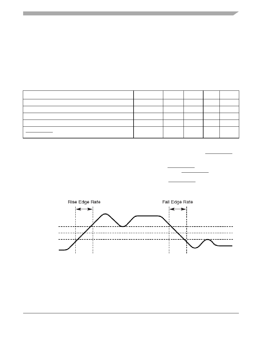
Figure 46. Differential Measurement Points for Rise and Fall Time
Table 52. SerDes Reference Clock Common AC Parameters
At recommended operating conditions with XCOREVDD= 1.0V ± 5%
Parameter
Symbol
Min
Max
Unit
Note
Rising Edge Rate
Rise Edge Rate
1.0
4.0
V/ns
2, 3
Falling Edge Rate
Fall Edge Rate
1.0
4.0
V/ns
2, 3
Differential Input High Voltage
VIH
+200
—
mV
2
Differential Input Low Voltage
VIL
—
–200
mV
2
Rising edge rate (SDn_REF_CLK) to falling edge rate
(SDn_REF_CLK) matching
Rise-Fall
Matching
—20
%
1, 4
Note:
1. Measurement taken from single ended waveform.
2. Measurement taken from differential waveform.
3. Measured from -200 mV to +200 mV on the differential waveform (derived from SDn_REF_CLK minus SDn_REF_CLK).
The signal must be monotonic through the measurement region for rise and fall time. The 400 mV measurement window is
centered on the differential zero crossing. See Figure 46.
4. Matching applies to rising edge rate for SDn_REF_CLK and falling edge rate for SDn_REF_CLK. It is measured using a
200 mV window centered on the median cross point where SDn_REF_CLK rising meets SDn_REF_CLK falling. The
median cross point is used to calculate the voltage thresholds the oscilloscope is to use for the edge rate calculations. The
Rise Edge Rate of SDn_REF_CLK should be compared to the Fall Edge Rate of SDn_REF_CLK, the maximum allowed
difference should not exceed 20% of the slowest edge rate. See Figure 47.
VIH = +200
VIL = –200
0.0 V
SDn_REF_CL
K
minus
相关PDF资料 |
PDF描述 |
|---|---|
| KMPC8314CVRAGDA | IC MPU POWERQUICC II 620-PBGA |
| KMPC8313ZQAFFB | IC MPU POWERQUICC II 516-PBGA |
| 2-1734798-7 | CONN HOUSING FPC 27POS R/A SMD |
| 487951-4 | 004 1MM FPC TOP HORZ |
| 3-487951-0 | CONN 1MM FPC 30POS R/A SMD |
相关代理商/技术参数 |
参数描述 |
|---|---|
| KMPC8314EVRAGDA | 功能描述:微处理器 - MPU ENCRYPT RoHS:否 制造商:Atmel 处理器系列:SAMA5D31 核心:ARM Cortex A5 数据总线宽度:32 bit 最大时钟频率:536 MHz 程序存储器大小:32 KB 数据 RAM 大小:128 KB 接口类型:CAN, Ethernet, LIN, SPI,TWI, UART, USB 工作电源电压:1.8 V to 3.3 V 最大工作温度:+ 85 C 安装风格:SMD/SMT 封装 / 箱体:FBGA-324 |
| KMPC8314VRAGDA | 功能描述:微处理器 - MPU NON-ENCRYPT RoHS:否 制造商:Atmel 处理器系列:SAMA5D31 核心:ARM Cortex A5 数据总线宽度:32 bit 最大时钟频率:536 MHz 程序存储器大小:32 KB 数据 RAM 大小:128 KB 接口类型:CAN, Ethernet, LIN, SPI,TWI, UART, USB 工作电源电压:1.8 V to 3.3 V 最大工作温度:+ 85 C 安装风格:SMD/SMT 封装 / 箱体:FBGA-324 |
| KMPC8315CVRAGDA | 功能描述:微处理器 - MPU NON-ENCRYPT RoHS:否 制造商:Atmel 处理器系列:SAMA5D31 核心:ARM Cortex A5 数据总线宽度:32 bit 最大时钟频率:536 MHz 程序存储器大小:32 KB 数据 RAM 大小:128 KB 接口类型:CAN, Ethernet, LIN, SPI,TWI, UART, USB 工作电源电压:1.8 V to 3.3 V 最大工作温度:+ 85 C 安装风格:SMD/SMT 封装 / 箱体:FBGA-324 |
| KMPC8315ECVRAGDA | 功能描述:微处理器 - MPU ENCRYPT RoHS:否 制造商:Atmel 处理器系列:SAMA5D31 核心:ARM Cortex A5 数据总线宽度:32 bit 最大时钟频率:536 MHz 程序存储器大小:32 KB 数据 RAM 大小:128 KB 接口类型:CAN, Ethernet, LIN, SPI,TWI, UART, USB 工作电源电压:1.8 V to 3.3 V 最大工作温度:+ 85 C 安装风格:SMD/SMT 封装 / 箱体:FBGA-324 |
| KMPC8315EVRAGDA | 功能描述:微处理器 - MPU ENCRYPT RoHS:否 制造商:Atmel 处理器系列:SAMA5D31 核心:ARM Cortex A5 数据总线宽度:32 bit 最大时钟频率:536 MHz 程序存储器大小:32 KB 数据 RAM 大小:128 KB 接口类型:CAN, Ethernet, LIN, SPI,TWI, UART, USB 工作电源电压:1.8 V to 3.3 V 最大工作温度:+ 85 C 安装风格:SMD/SMT 封装 / 箱体:FBGA-324 |
发布紧急采购,3分钟左右您将得到回复。